UNIT – 7
Memory Interface – 2, I/O Interface – 1
The 3-to-8 Line Decoder (74LS138)
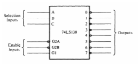
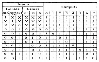
One of the more common, although not only, integrated circuit decoders found in many microprocessor-based systems is the 74LS138 3-to-8line decoder. The figure below shows this decoder and its truth table. The truth table shows that only one of the eight outputs ever goes low at any time. For any of the decoder's outputs to go low, the three enable inputs (G2A, G2B, and Gl) must all be active. To be active, the G2A and G2B inputs must both be low (logic 0), and G I must be high (logic 1). Once the 74LS138 is enabled, the address inputs (C, B, and A) select which output pin goes low. Imagine eight EPROM CE inputs connected to the eight outputs of the decoder! This is a very powerful device because it selects eight different memory devices at the same time.
|
Fig 1 3:8 Decoder
|
Fig 2 Truth Table for 3:8 Decoder
The Dual 2-to-4 Line Decoder (74LS139)
|
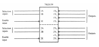
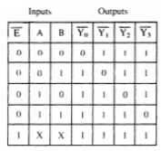
Fig 3 2 to 4line Decoder ad its Truth Table
PLD Programmable Decoders
Combinatorial Programmable Logic Arrays.
Initially, all of the fuses connect all of the vertical/horizontal connections. Programming is accomplished by blowing fuses to connect various inputs to the OR gate array. The wired-AND function is performed at each input connection that allows a product term of up to 16 inputs. A logic expression using the PAL16L8 can have 7 product terms with 16 inputs NORed together to generate the output expression. This device is ideal as a memory address decoder because of its structure. It is also ideal because the outputs are active low.
Key takeaway
When the 8088 microprocessor is compared to the 2716 EPROM, a difference in the number of address connections surfaces-the EPROM has 11 address connections and the microprocessor has 20. This means that the microprocessor sends out a 20-bit memory address whenever it reads or writes data.
Since the EPROM has only 11 address inputs, there is a mismatch that must somehow be corrected. If only 11 of the 8088's address pins are connected to the memory, then the 8088 will see only 2K bytes of memory instead of the 1M byte that it expects the memory to contain. The decoder corrects the mismatch by decoding the address pins that do not connect to the memory component.
Interfacing EPROM to the 8088
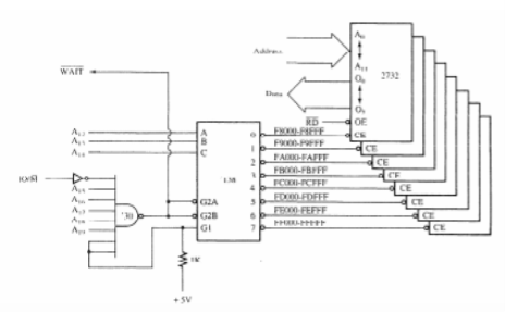
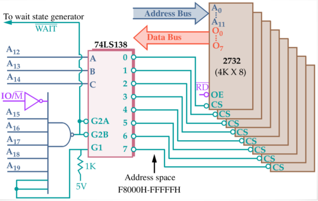
In order to correct this problem, we must add a NAND gate to generate a signal to enable the decoder and a signal for the wait state generator. With a wait state inserted every time this section of the memory is accessed, the 8088 will allow 660 ns for the EPROM to access data. Recall that an extra wait state adds 200 ns (1 clock) to the access time. The 660 ns is ample time for a 450 ns memory component to access data, even with the delays introduced by the decoder and any buffers added to the data bus.
|
Fig 4 8 EPROM interfaced to 8088-microprocessor
The decoder is selected for a memory address range that begins at location F8000H and continues through location FFFFFH-the upper 32K bytes of memory. This section of memory is an EPROM because FFFFOH is where the 8088 starts to execute instructions after a hardware reset. We often call location FFFFOH the cold-start location. The software stored in this section of memory would contain a JMP instruction at location FFFFOH that jumps to location F8000H so that the remainder of the program can execute.
|
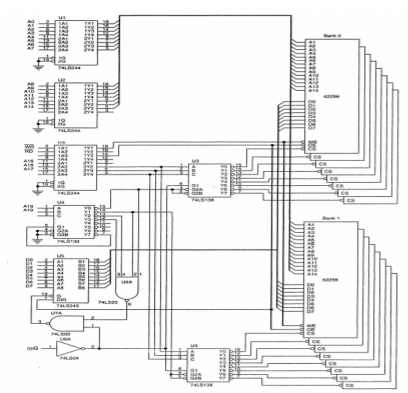
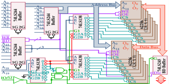
Fig 5 512k byte static memory using 16 62255 SRAMS
Also notice from the circuit in shown above that all the address inputs to this section of memory are buffered, as are the data bus connections and control signals RD and WR. Buffering is important when many devices appear on a single board or in a single system. Suppose that three other boards like this are plugged into a system. Without the buffers on each board, the load on the system address, data, and control buses would be enough to prevent proper operation. Buffers are normally used if the memory will contain additions at some future date. If the memory will never grow, then buffers may not be needed.
16-Bit Bus Control
|
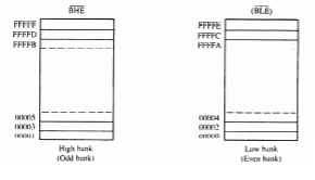
Fig 6 High and Low 8-bit Memory Banks
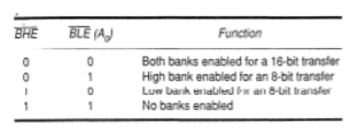
Table below depicts the logic levels on these two pins and the bank or banks selected. Bank selection is accomplished in two ways: (1) a separate write signal is developed to select a write to each bank of the memory or (2) separate decoders are used for each bank. As a careful comparison reveals, the first technique is by far the least costly approach to memory interface for the 8086, 80186, 80286, and 80386SX microprocessors.
|
Fig 7 Memory Bank Selection using BHE and BLE
Key takeaway
8088/80188 microprocessors have an 8-bit data bus, which makes them ideal to connect to common 8-bit memory devices available. For the 8088/80188 to function correctly with memory, however, the system must decode the address to select a memory component.
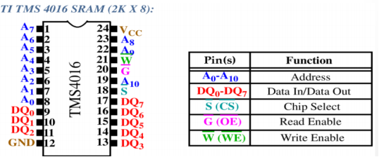
SRAM
- SRAMs are virtually identical to the EPROM with respect to the pinout although access time is faster (250ns).
- SRAMs used for caches have access times as low as 10ns.
|
Fig 8 SRAM Functional Block Diagram
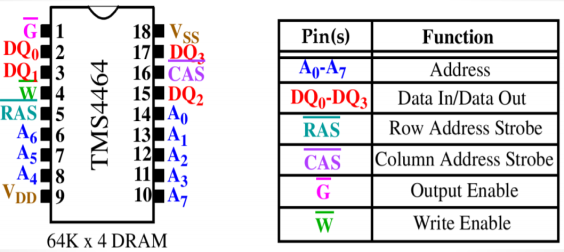
DRAM
- DRAMs are available in much larger sizes, e.g., 64M X 1.
- DRAMs MUST be refreshed (rewritten) every 2 to 4 ms Since they store their value on an integrated capacitor that loses charge over time.
- This refresh is performed by a special circuit in the DRAM which refreshes the entire memory.
|
Fig 9 DRAM Interfacing
System design based on memory and peripherals
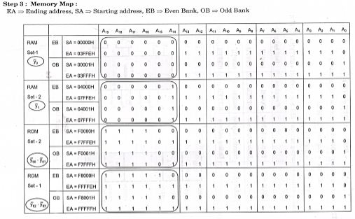
- Step 1: Total EPROM required = 64 KB
Chip size available = 16 KB
∴Number of chips required=64KB/16KB=4
∴Number of sets required=Number of chips Number of banks=42=2
- SET 1: Ending address of SET 1 = FFFFFH
SET size = Chip size x 2 = 16 KB x 2 = 32 KB
i.e. 00000011171111F1111F1111F00000011171111F1111F1111F
Starting address = Ending address – SET size=FFFFFH–07FFFH
- SET 2: Ending address of SET 2 = F7FFFH (previous ending - 1)
SET size = Chip size x 2 = 16 KB x 2 = 32 KB
i.e. 00000011171111F1111F1111F00000011171111F1111F1111F
Starting address = Ending address – SET size=F7FFFH–07FFFH=F0000H

- Step 2: Total RAM required = 32 KB
Chip size available = 8 KB
∴Number of chips required=32KB/8KB=4
∴Number of sets required=Number of chips Number of banks=42=2
- SET 1: Starting address = 00000H
SET size = Chip size x 2 = 8 KB x 2 = 32 KB
i.e. 00000001131111F1111F1111F00000001131111F1111F1111F
Ending address = Starting address – SET size=04000H+03FFFH=07FFFH
- SET 2: Starting address = 04000H (previous ending - 1)
SET size = Chip size x 2 = 8 KB x 2 = 32 KB
i.e. 00000001131111F1111F1111F00000001131111F1111F1111F
Ending address = Starting address – SET size=04000H–03FFFH=07FFFH

|
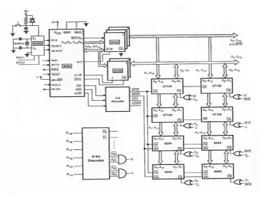
- Step 4: Final Implementation:
|
Fig 10 Final Implementation after interfacing
7.4.1 Introduction to I/O Interface
Whenever the 8086 executes an IN and OUT instruction to access a port, none of the segment registers are involved in producing the physical address sent out by the 8086. The port address is sent out directly from the 8086 on lines AD0- AD15, and 0’s is output on lines A16-A19. In an 8086 system which uses direct I/O, the M/IO (Active Low) signal is used to enable a memory decoder or a port decoder. You please remember that the M/IO (Active Low) signal being high was one of the enabling conditions for the memory decoding as we discussed previously. The opposite of this enables the port decoder. During the execution of an IN instruction, the RD (Active Low) signal from the 8086 will be low.
This signal can be used to enable an addressed input port device. During the execution of an OUT instruction the WR (Active Low) signal from the 8086 will be low. This signal can be used to enable an output port device. Since the 8086 microprocessor outputs up to 16-bit address for direct I/O operations, it can address any one of the 65536 input ports and any one of the 65536 output ports. However, to achieve this direct I/O, the 8086-microprocessor should be provided with the appropriated decoding circuitry
Key takeaways
Besides the 8086-microprocessor chip, an 8086 based microcomputer system includes memory, I/O devices and the interfacing circuits required to connect these devices to the 8086-microprocessor. There are two modes of operation for Intel 8086 namely the minimum mode and the maximum mode.
When only one 8086 CPU is to be used in a micro-computer system the 8086 is used in the minimum mode of operation. In a multi-processor system, it operates in the maximum mode. In the minimum mode, the 8086 CPU itself issues the control signals required by memory and I/O devices. In case of maximum mode of operation, control signals are issued by Intel 8288 bus controller which is used with 8086 for this purpose.
7.4.2 I/O Port Address Decoding.
The main difference between memory decoding and isolated I/0 decoding is the number of address pins connected to the decoder. We decode A 32-A0, A23-A0, or A 19-A0 for memory and A 15-A0 for isolated I/0. Sometimes, if the I/0 devices use only fixed I/0 addressing, we decode only A7-A0. Another difference is that we use the  and
and  to activate I/0 devices for a read or a write operation. On earlier versions of the microprocessor, I0/
 = 1 and
  or
or  are used to activate I/0 devices. On the newest versions of the microprocessor, the M/
 = 0 and
  are used to activate I/0 devices.
Decoding 8-Bit 1/0 Addresses
As mentioned, the fixed I/0 instruction uses an 8-bit l/0 port address that appears on A 15-A0 as OOOOH-OOFFH. If a system will never contain more than 256 I/0 devices, we often decode only address connections A7-A0 for an 8-bit 1/0 port address. Thus, we ignore address connections A 15-A8. Please note that the DX register can also address I/0 ports OOH-FFH. Also note that if the address is decoded as an 8-bit address, then we can never include 1/0 devices that use a 16-bit l/0 address.
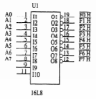
The 74ALS138 decoder that decodes 8-bit 1/0 ports FOH-F7H. (We assume that the system will only use I/0 ports OOH-FFH for this decoder.) This decoder is identical to a memory address decoder except we only connect address bits A7 -A0 to the inputs of the address lines (A15-A8) must be decoded.
|
Fig 11 Decoder that generates I/O port address of F0H-F7H
|
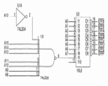
Fig 12 Decoder that Decodes EFF8H-EFFFH
Figure above a circuit that contains a PAL16L8 and an 8-input NAND gate used to decode I/0 ports EFF8H-EFFFH. These are common I/0 port assignments in a PC used for the serial communications port. The NAND gate decodes the first 8-bits of the I/0 port address (A 15-A8) so that it generates a signal to enable the PAL16L8 for any I/0 address between EFOOH and EFFFH.
Key takeaway
The main difference between memory decoding and isolated I/0 decoding is the number of address pins connected to the decoder. We decode A 32-A0, A23-A0, or A 19-A0 for memory and A 15-A0 for isolated I/0. Sometimes, if the I/0 devices use only fixed I/0 addressing, we decode only A7-A0
Reference:
1. Gaonkar, Ramesh S , “Microprocessor Architecture, Programming and Applications with 8085”, Penram International Publishing.
2. Ray A K, Bhurchandi K M, “Advanced Microprocessors and Peripherals”, TMH Hall D V, Microprocessor Interfacing’, TMH
3. Microprocessor & Interfacing by D.V hall,TMH
4. Brey, Barry B, “INTEL Microprocessors”, PHI
