UNIT 8
I/O Interface – 2, Interrupts, and DMA: I/O Interface
Pin Configuration
|
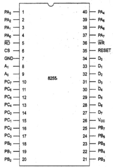
Fig.1: Pin Configuration of 8255
- It is also known as Programmable Peripheral Interface.
- It is a multi-port device.
- It has 24 I/O pins. They are divided into three 8 bit ports PA, PB, PC.
- Port A and port B are used as 8-bit I/O ports.
- Port C is used as an 8-bit I/O port or as two 4-bit I/O ports or produces handshake signals for ports A and B.
- CS: The chip select CS (pin 6) is used to enable the 8255 chip. It is an active-low signal, hence is enabled when CS = 0.
- RESET: It is an input pin 35 and is connected to the RESET line of system 8085. When the system is reset, all the ports behave as input lines. This is done to prevent 8255 from being destroyed due to mismatch of ports.
- Eight data lines (D0–D7) are available to read/write data into the ports or control register under the status of the RD (pin 5) and WR (pin 36), which are active-low signals for read and write operations respectively.
- Address lines A1 and A0 allow to access a data register for each port or a control register, as listed below:
A1 | A0 | PORT SELECTED |
0 | 0 | PORT A |
0 | 1 | PORT B |
1 | 0 | PORT C |
1 | 1 | Control Register |
Operating Modes
There are two basic operating modes of 8255.
- Bit set/reset mode (BSR mode)
- Input/ output mode (I/O mode)
The modes selected by the D7 bit of the control word register are:
When D7 = 1, 8255 operates in I/O mode else BSR mode.
BSR MODE
|
- D7 bit is always 0 for this mode.
- Bits D6, D5 and D4 are don't care bits.
- Bits D3, D2 and D1 are used for pin selection of Port C.
- Bit D0 is used to set/reset the above selected pin.
Selection of port C pin is determined as follows:
D3 | D2 | D1 | Bit/pin of port C selected |
0 | 0 | 0 | PC0 |
0 | 0 | 1 | PC1 |
0 | 1 | 0 | PC2 |
0 | 1 | 1 | PC3 |
1 | 0 | 0 | PC4 |
1 | 0 | 1 | PC5 |
1 | 1 | 0 | PC6 |
1 | 1 | 1 | PC7 |
For example:
If PC4 be set, then in the control word is,
- Since it is a BSR mode, D7 = '0'.
- Since D4, D5, D6 are don’t care hence assuming them to be '0'.
- PC4 has to be selected, hence, D3 = '1', D2 = '0', D1 = '0'.
- PC4 has to be set, hence, D0 = '1'.
Thus, as per the above values, 0AH (in hex) will be loaded into the Control Word Register (CWR).
I/O MODE
When D7 bit of the Control Word Register is 1, this mode is selected.
There are three I/O modes and they are:
- Mode 0 - Simple I/O
- Mode 1 - Strobed I/O
- Mode 2 - Strobed Bi-directional I/O
- Mode 0 – Simple or basic I/O mode:
Port A, B and C can work either as input or as output function. The outputs are latched but the inputs are not latched. It can handle interrupts.
- Mode 1 – Handshake or strobbed I/O:
Here, either port A or B can work and port C is used to provide handshake signals. The outputs as well as inputs are latched. It can handle interrupts. Before actual data is transmitted, there is transmission of signal to match speed of CPU and printer.
- Mode 2 – Bidirectional I/O:
In this mode only port A will work, port B can either is in mode 0 or 1 and port C bits are used as handshake signal. The outputs as well as inputs are latched. It has interrupt handling capability.
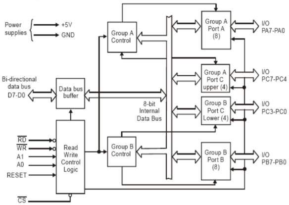
Functional block diagram
|
Fig 2 Functional Block Diagram
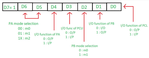
Control Word for I/O mode
|
- The most significant bit (D7) is 1 for the I/O mode.
- D6 & D5: It is used to set the port A mode.
|
- D4 : It is used to check whether port A is taking input or displaying the output. If it is 1 then input else output.
- D3: It is used to check whether port C higher bites takes input or output. If 1, then input else output.
- D2: It tells the mode of port B. If 0, then port B is in M0 mode else in M1 mode.
- D1: It is used to check whether port B is taking input or displaying output. If 1, then input else output.
- D0: It is used to tell whether port C lower bits is taking input or displaying output. If 1, then it takes input else displays output.
Key takeaway
When 8255 microprocessors are reset, it clears the control word register contents and sets all the ports to input mode. Used as keyboard and display interface, traffic light control, printer interface and so on.
Pin Configuration
|
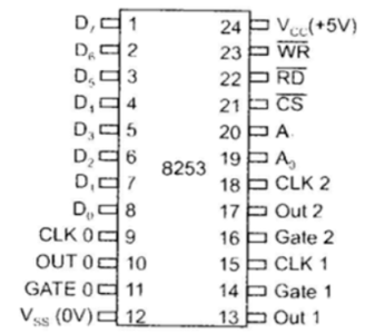
Fig.3: Pin Configuration of 8253
- It is a programmable counter / timer chip which is used as an Intel microcomputer peripheral.
- It uses nMOS technology with +5V supply and is packaged in a 24-pin plastic DIP.
- It is used as an event counter, elapsed time indicator, programmable one-shot etc.
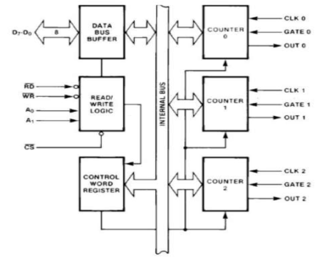
- There are three counters, a data bus buffer, Read/Write control logic, and a control register. Each counter has two input signals - CLOCK & GATE, and one output signal - OUT.
It is a tri-state, bi-directional, 8-bit buffer, which is used to interface the 8253 to the system data bus. It has three basic functions −
- Programming the modes of 8253.
- Loading the count registers.
- Reading the count values.
It includes 5 signals, i.e. RD, WR, CS, and the address lines A0 & A1. In the peripheral I/O mode, the RD and WR signals are connected to IOR and IOW and in the memory mapped I/O mode to MEMR and MEMW.
Address lines A0 & A1 of the CPU are connected to lines A0 and A1 of the 8253 and CS is tied to a decoded address.
A1 | A0 | Result |
0 | 0 | Counter 0 |
0 | 1 | Counter 1 |
1 | 0 | Counter 2 |
1 | 1 | Control Word Register |
X | X | No Selection |
Functional block diagram:
|
Fig 4 Block Diagram of 8253
Control Word Register
This register can be accessed when lines A0 & A1 are at logic 1.
It is used to write a command word, its mode and either a read or write operation.
Following table provides the result for various control inputs:
A1 | A0 | RD | WR | CS | Result |
0 | 0 | 1 | 0 | 0 | Write Counter 0 |
0 | 1 | 1 | 0 | 0 | Write Counter 1 |
1 | 0 | 1 | 0 | 0 | Write Counter 2 |
1 | 1 | 1 | 0 | 0 | Write Control Word |
0 | 0 | 0 | 1 | 0 | Read Counter 0 |
0 | 1 | 0 | 1 | 0 | Read Counter 1 |
1 | 0 | 0 | 1 | 0 | Read Counter 2 |
1 | 1 | 0 | 1 | 0 | No operation |
X | X | 1 | 1 | 0 | No operation |
X | X | X | X | 1 | No operation |
Operating Modes
8253 can be operated in 6 different modes. They are:
Mode 0 ─ Interrupt on Terminal Count
- It is used for generating an interrupt to the microprocessor after a certain interval.
- The output is low after the mode is set and remains LOW after the count value is loaded into the counter.
- The counter decrement continues till the terminal count is reached.
- The GATE signal remains high for normal counting. When it is low, counting is terminated and the current count is latched till it goes high again.
Mode 1 – Programmable One Shot
- It is used as a mono stable multi-vibrator.
- GATE is used as a trigger input in this mode.
- As the count is loaded the output remains high and a trigger is applied.
- The output is high after initialization.
- Whenever the count becomes zero, a low pulse is generated at the output and the counter is reloaded.
Mode 3 – Square Wave Generator
- This mode is same as Mode 2 except that the output remains low for half of the timer period and high for the next half of the period.
Mode 4 − Software Triggered Mode
- In this, the output remains high till the timer counts to zero and at this point the output is low and then goes high again.
- The count is latched when GATE LOW.
- As per the terminal count, for one clock cycle the output goes low then goes HIGH. The low pulse is used as a strobe.
Mode 5 – Hardware Triggered Mode
- This mode generates a strobe as a result to an externally generated signal.
- It is same as mode 4 except that the counting is initiated by a signal at the gate input.
- As soon as it is initialized, the output goes high.
- When the terminal count is reached, the output goes low for one clock cycle.
Key takeaway
- In free running counter applications.
- As an event counter.
- Rate generator.
- An interrupt is a condition that arises during the working of a microprocessor. The microprocessor services it by executing a subroutine called Interrupt Service Routine (ISR).
- There are three sources of interrupts for 8086:
Hardware interrupt-
These interrupts occur as signals on the external pins of the microprocessor. 8086 has two pins to accept hardware interrupts, NMI and INTR.
Software interrupt-
These interrupts occurs by writing the software interrupt instruction INT n where ‘n’ can be any value from 0 to 255 (00H to FFH). Hence all 256 interrupts can be invoked by software.
Error conditions (Exception or types)-
8086 is interrupted when some special conditions occur while executing certain instructions in the program. Example: An error in division automatically causes the INT 0 interrupt.
Interrupt Vector Table (IVT):
|
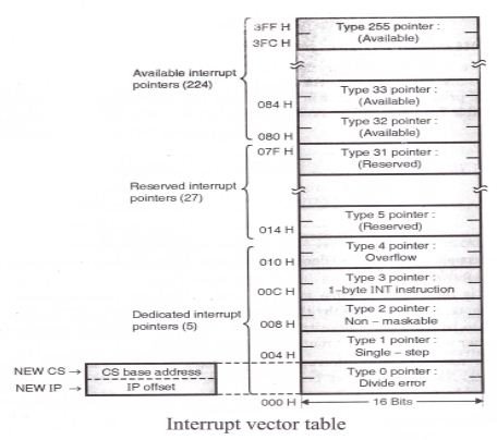
Fig 5 Interrupt Vector Table
- The interrupt vector (or interrupt pointer) table is the link between an interrupt type code and the procedure that has been designated to service interrupts associated with that code. 8086 supports total 256 types i.e. 00H to FFH.
- For each type of interrupt it has to reserve four bytes i.e. double word.
- The higher addressed word contains the base address of the segment and is normally referred as NEW CS.
- The lower addressed word consists of the procedure’s offset and is normally referred as NEW IP.
- Thus NEW CS provides new physical address from where user ISR routine will start.
- Here, four bytes (2 for NEW CS and 2 for NEW IP) are required; hence interrupt pointer table occupies up to the first 1k bytes (i.e. 256 x 4 = 1024 bytes) of lower order memory.
- The total interrupt vector table is divided into three groups namely,
A. Dedicated interrupts (INT 0…..INT 4)
B. Reserved interrupts (INT 5…..INT 31)
C. Available interrupts (INT 32…..INT 225)
Dedicated interrupts (INT 0…..INT 4):
- INT 0 (Divide Error)-
- This interrupt occurs whenever there is division error. This condition normally occurs when the divisor is very small as compared to the dividend or the divisor is zero.
- Its ISR address is stored at location 0 x 4 = 00000H in the IVT.
- INT 1 (Single Step)-
- The microprocessor executes this interrupt after every instruction if the TF is set.
- Its ISR displays contents for all registers. Its ISR address is stored at location 1 x 4 = 00004H in the IVT.
- INT 2 (Non mask-able Interrupt)-
- The microprocessor executes this ISR in response to an interrupt on the NMI (Non mask-able Interrupt) line.
- Its ISR address is stored at location 2 x 4 = 00008H in the IVT.
- INT 3 (Breakpoint Interrupt)-
- This interrupt causes breakpoints in the program. It occurs by writing the instruction INT 03H or simply INT.
- It is useful in debugging large programs.
- Its ISR is used to display the contents of all registers on the screen. Its ISR address is stored at location 3 x 4 = 0000CH in the IVT.
- INT 4 (Overflow Interrupt)-
- It occurs if the overflow flag is set and the microprocessor executes the INTO (Interrupt on Overflow) instruction.
- It detects overflow error in signed arithmetic operations.
- Its ISR address is stored at location 4 x 4 = 00010H in the IVT.
Reserved interrupts (INT 5…..INT 31):
These levels are reserved by Intel to be used in higher processors like 80386, Pentium etc. They are not available to the user.
Available interrupts (INT 32…..INT 225):
- These are user defined, software interrupts.
- ISRs are written by the users to service various user defined conditions.
- These interrupts are invoked by writing the instruction INT n.
- Its ISR address is obtained by the microprocessor from location n x 4 in the IVT.
Hardware Interrupts:
- NMI (Non mask-able interrupt)-
- This is a non-mask-able, edge triggered, high priority interrupt.
- On receiving this, the microprocessor executes INT instruction.
- Microprocessor obtains the ISR address from location 2 x 4 = 00008H from the IVT.
- It reads 4 locations starting from this address to get the values for IP and CS to execute the ISR.
- INTR-
- This is a mask-able, level triggered, low priority interrupt.
- On receiving an interrupt on INTR line, the microprocessor executes 2 INTA pulses.
- It is masked by making IF = 0 by software through CLI instruction.
- It is unmasked by making IF = 1 by software through STI instruction.
.
Interrupt processing and pre-defined interrupts
The first five interrupt types are reserved for specific functions.
Fig 6 Interrupts
- INT 0 (Divide Error)-
- This interrupt occurs whenever there is division error. This condition normally occurs when the divisor is very small as compared to the dividend or the divisor is zero.
- Its ISR address is stored at location 0 x 4 = 00000H in the IVT.
- INT 1 (Single Step)-
- The microprocessor executes this interrupt after every instruction if the TF is set.
- Its ISR displays contents for all registers. Its ISR address is stored at location 1 x 4 = 00004H in the IVT.
- INT 2 (Non mask-able Interrupt)-
- The microprocessor executes this ISR in response to an interrupt on the NMI (Non mask-able Interrupt) line.
- Its ISR address is stored at location 2 x 4 = 00008H in the IVT.
- INT 3 (Breakpoint Interrupt)-
- This interrupt causes breakpoints in the program. It occurs by writing the instruction INT 03H or simply INT.
- It is useful in debugging large programs.
- Its ISR is used to display the contents of all registers on the screen. Its ISR address is stored at location 3 x 4 = 0000CH in the IVT.
- INT 4 (Overflow Interrupt)-
- It occurs if the overflow flag is set and the microprocessor executes the INTO (Interrupt on Overflow) instruction.
- It detects overflow error in signed arithmetic operations.
- Its ISR address is stored at location 4 x 4 = 00010H in the IVT.
Key takeaway
Hardware interrupt-
These interrupts occur as signals on the external pins of the microprocessor. 8086 has two pins to accept hardware interrupts, NMI and INTR.
Software interrupt-
These interrupts occur by writing the software interrupt instruction INT n where ‘n’ can be any value from 0 to 255 (00H to FFH). Hence all 256 interrupts can be invoked by software.
- DMA is used for bulk data transfer from I/O devices to microprocessor or vice-versa.
- In this method I/O devices are allowed to transfer the data directly to the external memory without being routed through accumulator.
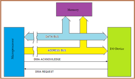
- The microprocessor relinquishes the control over the data bus and address bus, so that these can be used for transfer of data between the devices.
Working principle of direct memory access data transfer
- For this data transfer, a request to the microprocessor in form of HOLD signal, by the I/O device is sent.
- When microprocessor receives such request, it relinquishes the address and data buses and informs the I/O devices of the situation by sending Acknowledge signal HLDA.
- The I/O device then withdraws the request when the data transfer between the I/O device and external memory is complete.
|
Fig.7: DMA (Ref 3)
Reference:
1. Gaonkar, Ramesh S , “Microprocessor Architecture, Programming and Applications with 8085”, Penram International Publishing.
2. Ray A K, Bhurchandi K M, “Advanced Microprocessors and Peripherals”, TMH Hall D V, Microprocessor Interfacing’, TMH
3. Microprocessor & Interfacing by D.V hall,TMH
4. Brey, Barry B, “INTEL Microprocessors”, PHI
