- Instruction Set Processor (ISP)
- Central Processing Unit (CPU)
- A typical computing task consists of a series of steps specified by a sequence of machine instructions that constitute a program.
- An instruction is executed by carrying out a sequence of more rudimentary operations.
- The processor fetches one instruction at a time and performs the operation specified.
- Instructions are fetched from successive memory locations until a branch or a jump instruction is encountered.
- The processor keeps track of the address of the memory location containing the next instruction to be fetched using Program Counter (PC).
- Instruction Register (IR)
- Fetch the contents of the memory location pointed to by the PC.
- The contents of this location are loaded into the IR (fetch phase).
- IR ← [[PC]]
- Assuming that the memory is byte addressable, increment the contents of the PC by 4 (fetch phase).
- PC ← [PC] + 4
- Carry out the actions specified by the instruction in the IR (execution phase).
Executing an Instruction
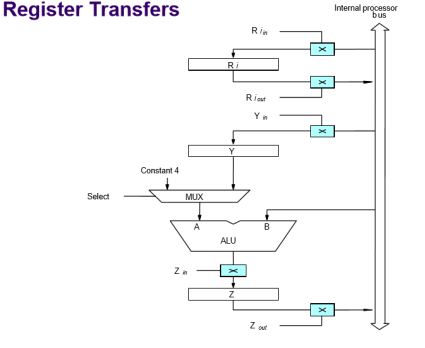
Transfer a word of data from one processor register to another or to the ALU.
Perform an arithmetic or a logic operation and store the result in a processor register.
Fetch the contents of a given memory location and load them into a processor register.
Store a word of data from a processor register into a given memory location.
|
Fig 1 – Register transfer
All operations and data transfers are controlled by the processor clock
Performing an Arithmetic or Logic Operation
The ALU is a combinational circuit that has no internal storage.
- ALU gets the two operands from MUX and bus. The result is temporarily stored in register Z.
- What is the sequence of operations to add the contents of register R1 to those of R2 and store the result in R3?
- R1out, Yin
- R2out, SelectY, Add, Zin
- Zout, R3in
- Address into MAR; issue Read operation; data into MDR.
- The response time of each memory access varies (cache miss, memory-mapped I/O…).
- To accommodate this, the processor waits until it receives an indication that the requested operation has been completed (Memory-Function-Completed, MFC).
- Move (R1), R2
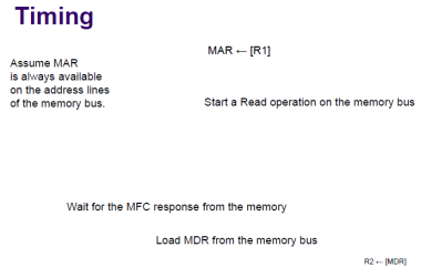
- MAR ← [R1]
- Start a Read operation on the memory bus
- Wait for the MFC response from the memory
- Load MDR from
- R1out, MARin, Read
- MDRinE, WMFC
- MDRout, R2in
Basic Processing Unit
Timing of Basic Processing Unit
|
Fig 2 - Timing
The figure represents Timing of a memory Read operation.
Assume MAR is always available on the address lines of the memory bus.
Execution of a Complete Instruction
- Add (R3), R1
- Fetch the instruction
- Fetch the first operand (the contents of the memory location pointed to by R3)
- Perform the addition
- Load the result into R1
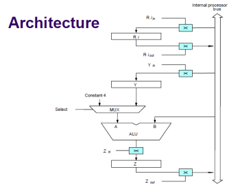
Architecture of Basic Processing Unit
|
Fig 3 - Architecture
Execution of a Complete Instruction
- Add (R3), R1
- M DRinE, WMFC
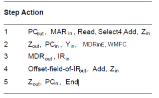
Control Sequencer execution of the instruction Add (R3),R1.
Execution of Branch Instructions in Basic Processing Unit
- A branch instruction replaces the contents of PC with the branch target address, which is usually obtained by adding an offset X given in the branch instruction.
- The offset X is usually the difference between the branch target address and the address immediately following the branch instruction.
- Conditional branch
|
Multiple-Bus Organization
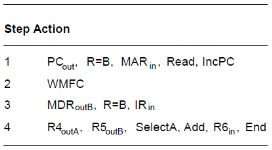
- Add R4, R5, R6
|
Key takeaways
- Instruction Set Processor (ISP)
- Central Processing Unit (CPU)
- A typical computing task consists of a series of steps specified by a sequence of machine instructions that constitute a program.
- An instruction is executed by carrying out a sequence of more rudimentary operations.
Registers Involved In Each Instruction Cycle:
- Memory address registers (MAR): It is connected to the address lines of the system bus. It specifies the address in memory for a read or write operation.
- Memory Buffer Register (MBR): It is connected to the data lines of the system bus. It contains the value to be stored in memory or the last value read from the memory.
- Program Counter (PC): Holds the address of the next instruction to be fetched.
- Instruction Register (IR): Holds the last instruction fetched.
The Instruction Cycle –
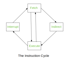
Each phase of Instruction Cycle can be decomposed into a sequence of elementary micro-operations. In the above examples, there is one sequence each for the Fetch, Indirect, Execute and Interrupt Cycles.
|
Fig 4 – Instruction Cycle
The Indirect Cycle is always followed by the Execute Cycle. The Interrupt Cycle is always followed by the Fetch Cycle. For both fetch and execute cycles, the next cycle depends on the state of the system.
|
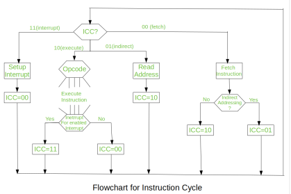
Fig 5 – Flowchart of instruction cycle
We assumed a new 2-bit register called Instruction Cycle Code (ICC). The ICC designates the state of processor in terms of which portion of the cycle it is in:
00 : Fetch Cycle |
At the end of each cycle, the ICC is set appropriately. The above flowchart of Instruction Cycle describes the complete sequence of micro-operations, depending only on the instruction sequence and the interrupt pattern(this is a simplified example). The operation of the processor is described as the performance of a sequence of micro-operation.
Different Instruction Cycles:
The Fetch Cycle –
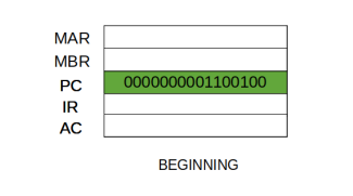
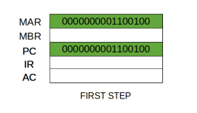
At the beginning of the fetch cycle, the address of the next instruction to be executed is in the Program Counter (PC).
|
Step 1: The address in the program counter is moved to the memory address register(MAR), as this is the only register which is connected to address lines of the system bus.
|
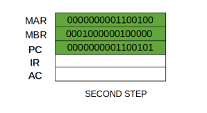
Step 2: The address in MAR is placed on the address bus, now the control unit issues a READ command on the control bus, and the result appears on the data bus and is then copied into the memory buffer register (MBR). Program counter is incremented by one, to get ready for the next instruction. (These two actions can be performed simultaneously to save time)
|
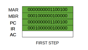
Step 3: The content of the MBR is moved to the instruction register(IR).
|
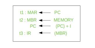
Thus, a simple Fetch Cycle consist of three steps and four micro-operation. Symbolically, we can write these sequence of events as follows:
|
Here ‘I’ is the instruction length. The notations (t1, t2, t3) represents successive time units. We assume that a clock is available for timing purposes and it emits regularly spaced clock pulses. Each clock pulse defines a time unit. Thus, all time units are of equal duration. Each micro-operation can be performed within the time of a single time unit. First time unit: Move the contents of the PC to MAR.
Second time unit: Move contents of memory location specified by MAR to MBR. Increment content of PC by I. Third time unit: Move contents of MBR to IR.
Note: Second and third micro-operations both take place during the second time unit.
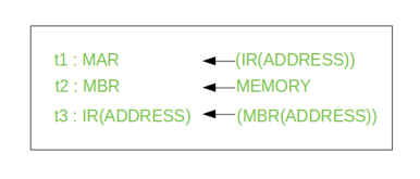
The Indirect Cycles –
Once an instruction is fetched, the next step is to fetch source operands. Source Operand is being fetched by indirect addressing (it can be fetched by any addressing mode, here it’s done by indirect addressing). Register-based operands need not be fetched. Once the opcode is executed, a similar process may be needed to store the result in main memory. Following micro-operations takes place:
|
Step 1: The address field of the instruction is transferred to the MAR. This is used to fetch the address of the operand.
Step 2: The address field of the IR is updated from the MBR.(So that it now contains a direct addressing rather than indirect addressing)
Step 3: The IR is now in the state, as if indirect addressing has not been occurred.
Note: Now IR is ready for the execute cycle, but it skips that cycle for a moment to consider the Interrupt Cycle.
The Execute Cycle
The other three cycles (Fetch, Indirect and Interrupt) are simple and predictable. Each of them requires simple, small and fixed sequence of micro-operation. In each case same micro-operation are repeated each time around.
Execute Cycle is different from them. Like, for a machine with N different opcodes there are N different sequence of micro-operations that can occur.
Let’s take an hypothetical example:
consider an add instruction:
|
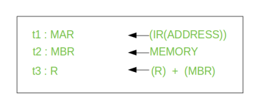
Here, this instruction adds the content of location X to register R. Corresponding micro-operation will be:
|
We begin with the IR containing the ADD instruction.
Step 1: The address portion of IR is loaded into the MAR.
Step 2: The address field of the IR is updated from the MBR, so the reference memory location is read.
Step 3: Now, the contents of R and MBR are added by the ALU.
Let’s take a complex example:

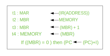
Here, the content of location X is incremented by 1. If the result is 0, the next instruction will be skipped. Corresponding sequence of micro-operation will be:
|
Here, the PC is incremented if (MBR) = 0. This test (is MBR equal to zero or not) and action (PC is incremented by 1) can be implemented as one micro-operation.
Note: This test and action micro-operation can be performed during the same time unit during which the updated value MBR is stored back to memory.
The Interrupt Cycle:
At the completion of the Execute Cycle, a test is made to determine whether any enabled interrupt has occurred or not. If an enabled interrupt has occurred then Interrupt Cycle occurs. The nature of this cycle varies greatly from one machine to another.
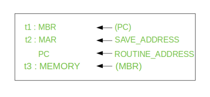
Let’s take a sequence of micro-operation:
|
Step 1: Contents of the PC is transferred to the MBR, so that they can be saved for return.
Step 2: MAR is loaded with the address at which the contents of the PC are to be saved.
PC is loaded with the address of the start of the interrupt-processing routine.
Step 3: MBR, containing the old value of PC, is stored in memory.
Note: In step 2, two actions are implemented as one micro-operation. However, most processor provide multiple types of interrupts, it may take one or more micro-operation to obtain the save_address and the routine_address before they are transferred to the MAR and PC respectively.
Key takeaways
- Memory address registers (MAR): It is connected to the address lines of the system bus. It specifies the address in memory for a read or write operation.
- Memory Buffer Register (MBR): It is connected to the data lines of the system bus. It contains the value to be stored in memory or the last value read from the memory.
- Program Counter (PC): Holds the address of the next instruction to be fetched.
- Instruction Register (IR): Holds the last instruction fetched.
All computing devices, from smartphones to supercomputers, pass data back and forth along electronic channels called "buses." You can think about the buses like freeways, in that having additional buses makes it easier to quickly transfer data, in the same way having more freeways or additional lanes increases the speed of traffic. In short, the number and type of buses used strongly affect the machine's overall speed. Simple computer designs move data with a single bus structure; multiple buses, however, vastly improve performance. In a multiple-bus architecture, each pathway is suited to handle a particular kind of information, detailed by BBC Bitesize.
Multiple Bus Organization Improves Efficiency
In a single-bus architecture, all components including the central processing unit, memory and peripherals share a common bus. When many devices need the bus at the same time, this creates a state of conflict called bus contention; some wait for the bus while another has control of it. The waiting wastes time, slowing the computer down, as Engineering 360 explains. Multiple buses permit several devices to work simultaneously, reducing time spent waiting and improving the computer's speed. Performance improvements are the main reason for having multiple buses in a computer design.
Additional Buses Allow Expansion
Having multiple buses available gives you more choices for connecting devices to your computer, as hardware makers may offer the same component for more than one bus type. As Digital Trends points out, most desktop PCs use the Serial Advanced Technology Attachment interface for internal hard drives, but many external hard drives and flash drives connect via USB. If your computer's SATA connections are all used, the USB interface lets you connect additional storage devices.
More Buses Means More Compatibility
As with all of a computer's components, bus designs evolve, with new types being introduced every few years. For example, the PCI bus that supports video, network and other expansion cards predates the newer PCIe interface, and USB has undergone several major revisions. Having multiple buses that support equipment from different eras lets you keep legacy equipment such as printers and older hard drives and add newer devices as well.
Multi-Core Requires Multiple Buses
A single central processing unit places heavy demands on the bus that carries memory data and peripheral traffic for hard drives, networks and printers; since the mid-2000s, however, most computers have adopted a multi-core model that require additional buses. To keep each core busy and productive, the new bus designs ferry increased amounts of information in and out of the microprocessor, keeping wait times to a minimum.
Intel's Core i5 microprocessor family, introduced in September 2009 and intended for business PCs, has performance technology that fits between the i3 and i7 series chips. The i5 is actually two processor lines, one for desktops and an energy-saving design for mobile computers. The i5 has many of the i7's speed-enhancing features, including multiple cores, Hyper-Threading and Turbo Boost.
The majority of modern microprocessor chips, the i5 included, employ a strategy of having more than one central processor core. This lets the computer run multiple processes at the same time, boosting the system's overall performance. The current lineup of i5 processors as of September 2012 has two cores, each of which run between 1.07 GHz to 2.8 GHz, depending on the particular model.
All of the i5 series processors have Hyper-Threading technology. This technology enables a second process to run on a core if the first process is waiting for data. The core's attention alternates between the two processes. This keeps both cores on the i5 as busy as possible and lets the chip finish tasks with greater speed.
The i5 has Intel's Turbo Boost, which is designed to maximize both performance and energy efficiency. During periods of peak demand, Turbo Boost increases the chip's clock speed while monitoring its temperature for safety. When the processor becomes idle, the technology reduces the clock speed, reducing the temperature and saving energy.
Virtualization enables the i5 to run multiple operating systems at the same time. With virtualization, a computer can act as many computers, all running different configurations of Microsoft Windows. This technology has helped companies with large computing facilities to consolidate functions onto one physical computer that formerly took several.
The cores in the i5 use a technology called Direct Media Interface to communicate with memory and other parts of the computer. DMI passes data through four data lanes each at a rate of 2.5 gigatransfers per second, or a total of 10 gigabits per second. Though this is faster than the Front Side Bus found in earlier microprocessors, it's not as fast as the Quickpath Interconnect found in some i7 processor models which transfer data up to 25.6GB per second.
Given the string of alphabet soup characters that identify expansion slots on modern computers, choosing the right graphics card for your business computer can be a confusing process. Standard office applications can be run on any basic graphics card; but specialized, graphic-intensive applications, such as drafting and animation software, may only work with certain types of cards. A little background knowledge on computer graphic technology and terminology can help to simplify the selection process.
Industry Standard Architecture slots were once standard on all PCs. This older slot has all but disappeared on modern motherboards. With a maximum data throughput of 2 to 3 megabytes per second, this slower slot supports only basic graphic capabilities and performance degrades rapidly at higher resolutions. Graphics cards utilizing ISA slots addressed system memory though the central processing unit, or CPU, resulting in slower overall system speed during graphic-intensive processes.
Peripheral Component Interconnect slots replaced ISA slots as an expansion interface standard in the early 1990s. PCI slots are engineered to allow a card's graphic processing unit (GPU) to bypass the computer's CPU entirely when addressing memory. This, combined with a throughput rate of up to 132 megabytes per second, provided a substantial improvement in performance over the ISA standard.
One bottleneck common to both ISA and PCI slots is the need to share a communications path with other expansion slots on the board. Accelerated Graphics Port slots streamline communication between the GPU and memory by eliminating the shared path. This direct path allows the GPU to run at higher clock speeds than are possible with standard ISA or PCI slots. Motherboards can only support one AGP slot, so if additional graphics cards are required, they must be installed in other slot types on the motherboard. AGP expansion cards are available in four versions: 1X, 2X, 4X and 8X. AGP-8X is the fastest, with a transfer rate of 2,100 megabytes per second. The cards are also available in three slot configurations designed to be powered from the motherboard by 1.5 volts, 3.3 volts or both. Not all AGP cards will work on all AGP motherboards so care must be taken when purchasing these graphics cards.
The latest development in graphic-card slots is PCI Express. The main difference between PCI Express and the older PCI slot is the elimination of bus or communication channel sharing. PCI Express utilizes dedicated serial links for each slot. These slots are available in four configurations: PCI-Ex1, PCI-Ex4, PCI-Ex8 and PCI-Ex16. A PCI Express x16 card on a fully supported motherboard boasts a simultaneous read/write speed of 4 gigabytes per second. As with AGP slots, PCI Express slots are designed to accept only matching cards. Consulting your system documentation before purchasing a new graphics card to check compatibility is always a wise move.
PCI-Express, commonly referred to as PCI-E, and PCI-X are both technology standards designed to improve upon the older PCI standard. Despite the similarity of their names, these two standards are incompatible with each other and handle the communication between peripherals and a computer system in very different ways.
Peripheral Component Interconnect, or PCI, was initially developed by Intel in the early 1990s as a standard for dealing with how peripheral devices communicate with the rest of the PC. Over the next few years, most of the rest of the computer industry adopted the technology, making PCI an industry-wide standard. In the late 1990s, the PCI Special Interest Group developed PCI-eXtended, which is a slightly more advanced version of PCI. A few years later, the group developed PCI-Express, which tackled the issue of peripheral communication in an entirely different way.
PCI-X, like the original PCI standard, is a shared bus technology, with all connected peripherals using the same bus in parallel. This means that as peripherals need to communicate with the computer, they often have to wait for their turn on the bus and as more devices require the bus, the peripheral's overall performance goes down. In contrast, PCI-E uses point-to-point technology, giving each individual peripheral its own dedicated bus. While each PCI-E bus is technically smaller than the shared bus of PCI-X, since each device doesn't have to wait for others that are using the bus, the end result is a much more efficient bus system.
The amount of data that can be transmitted over a PCI-X bus, otherwise known as the bus's bandwidth, is limited by the size of the physical bus and the speed at which it runs. Most PCI-X buses are 64-bits and run at either 100MHz or 133MHz, allowing for a maximum transmission speed of 1,066 MB per second. Advances in PCI-X technology have allowed for theoretical speeds up to 8.5GB per second, although speeds that high have some issues with interference. Additionally, PCI-X speeds are always lower then the maximum if you have more than one device using the bus.
Since PCI-E uses point-to-point technology, the only thing limiting the speed is how many lanes each connection has. PCI-E technology can support between one and 32 lanes, and runs at speeds beginning at 500 MB per second, up to a theoretical maximum of 16GB per second. Additionally, since PCI-E doesn't have the data overhead required to manage different connections like PCI-X does, the true data rate ends up being higher even in situations where the theoretical speeds would be the same.
PCI-E and PCI-X standards differ greatly when it comes to the size of the slot on the computer's motherboard. PCI-X slots are the same as the original PCI slots, although with one additional extension allowing for 64-bit communication. This means that these slots, and the corresponding peripheral cards, take up quite a bit of space on the motherboard. However, using these types of slots allow PCI-X slots to accept all but the oldest PCI cards. In contrast, PCI-E slots are completely different from PCI slots, and cannot accept any cards other those specifically designed for these slots. Additionally, the size of the slot is dependent on how many lanes the PCI-E bus has. A PCI-E x1 slot, which has just one lane, takes up almost no space on the motherboard, while a PCI-E x32 slot has 32 lanes, and is similar in size to PCI-X slots.
One of the most significant elements of a modern computer is the graphics card. The graphics card varies significantly -- from basic models barely capable of rendering advanced graphic elements in Windows, to massive workhorses used to enable the real-time rendering and development of cinema-quality 3D models. The exact location of the graphics card depends on the type of card in your computer.
The most difficult-to-find graphics card is not, in fact, a card at all. Many motherboard manufacturers embed the graphics card within the motherboard. These solutions allow a computer builder to get a PC running without considering graphics card compatibility. The graphics card is actually a single chip on the motherboard. Unlike discrete video cards, onboard cards share memory with the system. This makes onboard cards more cost-effective, but generally less powerful.
When a discrete graphics card is installed, it is typically located in the expansion slot closest to the CPU. Its location relates to the high-speed connection that motherboard manufacturers want between the CPU and the graphics card. This allows the graphics to take precedence over peripherals which demand fewer resources, such as sound cards or network adapters.
Two companies currently implement a system installing multiple graphics cards in a single machine. AMD and Nvidia offer Crossfire and Scalable Link Interface, respectively. You can identify a dual-card configuration by the bridge or cable link between two identical-looking cards within the PC.
Old expansion cards used the same ISA and PCI connections as sound or other peripheral cards. Today, graphics cards often utilize expansion slots on the motherboard specifically designed to meet the higher demands a graphics card places on the system bus. In the early 2000s, the accelerated graphics port, or AGP, appeared on motherboards to accommodate graphics cards only. AGP has now been largely replaced by a new, open standard known as PCI Express. PCI Express slots come in various speeds and can work with non-graphics cards. The fastest slots, however, typically reside closest to the CPU in anticipation of their use with graphics cards.
Today, even budget, commodity desktop PCs bought at an office supply store or discount retailer can be very efficient and powerful business productivity tools. Some users, however, require more computing power than a standard desktop computer can provide. These users often pay premium prices for high-end, built to order machines called workstations. Although desktop PCs and workstations can look the same on the outside, they are engineered to meet different user demands and expectations on the inside.
Desktop PCs are well-suited for home or small business computer users. Desktop PC users can surf the Web, play media files, email, play games, chat and video conference. Desktop PCs can also run office productivity software like databases, spreadsheets, word processors and Web applications with ease. Workstation users on the other hand, are often scientists, engineers, architects and digital media content creators whose work requires much more computing power than the average small business computer user would ever need.
Entry-level desktop, notebook and netbook computers today have more raw processing and storage capacity than many high-end workstations had a decade ago. Nevertheless, today's workstations are engineered to outperform desktops in data analysis, image manipulation and data transfer. The speed difference between a workstation and a desktop may not be obvious, however, when running a word processor application or Web browser. A workstation's superior performance can best be seen when you need to encode and render images or video files, search through massive databases, recalculate large spreadsheets, manipulate computer-aided design drawings or run multiple large applications simultaneously.
Each component in a workstation computer selected and optimized with the goal of increasing the movement of data into, within and out of the system. Workstations have more powerful graphics processing units for fast 2D or 3D graphic image creation and manipulation. While many new desktops have multi-core processors, workstations may come with more cores per CPU or support multiple, separate CPUs for even more parallel processing capability. In addition, workstations often come standard with more RAM and larger, faster hard drives than the typical desktop has.
Many desktops today come with their GPU, hard drive controllers and network interfaces built into the motherboard. In addition, you may not have the room or the connections available to add an additional hard drive or a better graphics card. Workstations, on the other hand, are often designed from the ground up to make it easy to add or swap hard drives, increase RAM, replace a graphics card or add additional graphics cards support multiple displays.
Most of Intel's microprocessor chips have a feature the company calls "hyper-threading." The technology improves performance in complex software environments by more efficiently juggling multiple program tasks. In essence, it wrings additional performance out of the central processing unit cores in a microprocessor by keeping them as busy as possible.
PCs hold many programs in memory at the same time. For traditional application programs, each constitutes one task. More modern programs, however, can consist of multiple tasks, called threads, all of which are independent of one another. For example, a Web browser program may have three tabs open, displaying different sites. Each tab has its own thread in memory, so downloads and other prolonged activities in one tab can continue working while you use another.
A processor with hyper-threading actively executes twice as many threads as an equivalent non-hyper-threaded model. It does this by having two copies of components that keep track of the CPU's state, allowing the CPU to rapidly switch back and forth between two threads. When the CPU needs data or programming instructions from memory, it waits a few millionths of a second for the computer to retrieve the information; in this brief interval, the CPU could be executing dozens of instructions. Hyper-threading cuts this wasted time by running instructions from another thread during the waiting period. Intel claims that this improves overall processor throughput by 30 percent.
Although hyper-threading allows each core to run two threads, it duplicates only certain memory elements, not all of the components in the CPU. The processor chip gains efficiency while increasing the chip die size by only 5 percent. The added cost to the chip is minor relative to the improvement in speed. Hyper-threading technology involves only the microprocessor chip itself and requires no external components.
As of July 2013, hyper-threading is available on Core i3, i5 and i7 processors; however, it made an early appearance on the Pentium 4, a single-core chip. Hyper-threading works equally well regardless of how many cores the chip has, as each receives the same performance benefit.
Motherboards are the backbone of a computer, holding different vital parts such as the processor, RAM and also providing connections to other peripherals. Upgrading internal computer parts is always an option if programs on your computer are running sluggishly or if software is incompatible due to a lack of resources. This can be especially true if you require high-end graphics or video editing programs. To upgrade you will need to know the types of slots on the motherboard and whether replacement parts will fit.
The CPU is often called the brains of a computer because it is the hardware that carries out instructions from software by using math, input/output commands and logic. The CPU slot (also known as a CPU socket) is where the processor is stored on a computer's motherboard. To replace a CPU you will need to raise the socket by lifting a small lever on the side of the socket; then you can gently pull out the CPU hardware. Replace the old CPU with a new one by aligning your new CPU with the socket, gently placing it in (do not push) and then flipping the socket lever to secure it.
Random access memory (RAM) is data storage hardware on your computer's motherboard. Despite the name, RAM does not actually "remember" anything when a computer is turned off. Programs must be saved on the hard drive or another storage device. In practical terms, RAM determines how many programs can run at once and how large the programs can be. Computers cannot run without RAM installed. They often come packaged with multiple strips located in RAM slots on the motherboard that are easily removable and replaceable. Upgrading RAM will improve the speed of your computer.
The Peripheral Component Interconnect (PCI) slot is a slot for expansion devices. Most desktop computers come with several PCI expansion slots. PCI slots are used for a variety of devices: modems, network cards, television tuners, radio tuners, video cards and sound cards, among others. Most computers today have several of these cards already built in. For computers that do not, these expansion devices provide additional functionality to a computer, making it possible for essential functions in a business such as wireless Internet connectivity.
The PCI Express slot, like the PCI slot, is used for expansion cards. PCI Express allows for higher transfer speeds than PCI and is therefore preferred for graphics cards. The PCI Express has replaced the Accelerated Graphics Port (AGP) in most computers as the primary slot for graphics cards. Many newer programs, such as Adobe's popular photo and video editors, rely more on an advanced graphics card to process data. Upgrading your graphics card can improve performance markedly.
A Graphics Processing Unit is a chip that handles any functions relating to what displays on your computer's screen. Every computer today has some form of GPU. A new GPU can speed up your computer, but the extent to which it accomplishes that acceleration has many variables. To understand whether a GPU will speed up your computer, first understand the role it plays.
Separate chips for graphics have existed as far back as the late 1970s, beginning with consoles such as the RCA “Pixie.” The modern understanding of a GPU, however, stems from a time when PCs began using graphical user interfaces. Before the GPU, all data flowed through the main processor -- data related to the function a program was performing, along with the graphical data the program was using to show you those functions. A bottleneck developed, especially with the rise in popularity of 3-D games. GPUs and video cards marketed as 3-D were added to handle all of the graphics-related processing, such as 3-D rendering, leaving the CPU to handle more complicated physics. In this way, GPUs have always enabled computers to run faster by virtue of not bogging down the CPU.
Perhaps the greatest speed advantage comes from replacing an onboard GPU solution with a new GPU. A motherboard that includes a graphics processor is said to have an onboard GPU. Just like a CPU, a GPU needs access to random access memory, or RAM, to function. In addition to generally having slower clock speeds, onboard graphics cards dedicate a portion of the system RAM to its graphics functions. Buying a separate GPU card not only gives you a potentially faster GPU, but also brings with it its own set of video RAM, or VRAM. Both graphics processing and multitasking will see a boost.
Replacing or Upgrading an Existing GPU
When your computer already has a separate GPU, performance comes from increasing the power. Like CPUs, GPUs are measure both by their clock speed, the amount of VRAM included, and the speed at which the GPU and VRAM can communicate. Other factors include the number of pixel pipelines and the supported graphics libraries. You’ll see a performance improvement throughout modern, graphics-intensive operating system by upgrading your card, but this will be primarily limited to interaction. Dragging a window in which a video is playing, for example, won’t cause that video to stutter, and clicking on a menu may animate more smoothly. The biggest performance increases, at this point, are seen in computer games which utilize 3-D graphics libraries such as OpenGL or Direct3D.
For extreme gamers, there’s option to install two graphics cards at once. Referred to as Crossfire with AMD and SLI through Nvidia, these proprietary technologies allow multiple graphics cards to work together simultaneously, much like a multicore CPU. The benefits of adding an additional GPU are largely limited to computer games, as the technology relates to separating 3-D rendering and physics calculations. Multiple GPUs can also help specific graphics-based programs, such as video-editing software.
Key takeaways
- All computing devices, from smartphones to supercomputers, pass data back and forth along electronic channels called "buses." You can think about the buses like freeways, in that having additional buses makes it easier to quickly transfer data, in the same way having more freeways or additional lanes increases the speed of traffic. In short, the number and type of buses used strongly affect the machine's overall speed. Simple computer designs move data with a single bus structure; multiple buses, however, vastly improve performance. In a multiple-bus architecture, each pathway is suited to handle a particular kind of information, detailed by BBC Bitesize.
The Control Unit is classified into two major categories:
- Hardwired Control
- Microprogrammed Control
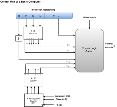
The Hardwired Control organization involves the control logic to be implemented with gates, flip-flops, decoders, and other digital circuits.
The following image shows the block diagram of a Hardwired Control organization.
|
Fig 6 – Control unit of a basic computer
- A Hard-wired Control consists of two decoders, a sequence counter, and a number of logic gates.
- An instruction fetched from the memory unit is placed in the instruction register (IR).
- The component of an instruction register includes; I bit, the operation code, and bits 0 through 11.
- The operation code in bits 12 through 14 are coded with a 3 x 8 decoder.
- The outputs of the decoder are designated by the symbols D0 through D7.
- The operation code at bit 15 is transferred to a flip-flop designated by the symbol I.
- The operation codes from Bits 0 through 11 are applied to the control logic gates.
- The Sequence counter (SC) can count in binary from 0 through 15.
Micro-programmed Control
The Microprogrammed Control organization is implemented by using the programming approach.
In Microprogrammed Control, the micro-operations are performed by executing a program consisting of micro-instructions.
The following image shows the block diagram of a Microprogrammed Control organization.
|
Fig 7 – Microprogrammed control unit of a basic computer
- The Control memory address register specifies the address of the micro-instruction.
- The Control memory is assumed to be a ROM, within which all control information is permanently stored.
- The control register holds the microinstruction fetched from the memory.
- The micro-instruction contains a control word that specifies one or more micro-operations for the data processor.
- While the micro-operations are being executed, the next address is computed in the next address generator circuit and then transferred into the control address register to read the next microinstruction.
- The next address generator is often referred to as a micro-program sequencer, as it determines the address sequence that is read from control memory.
Key takeaways
- The Control Unit is classified into two major categories:
- Hardwired Control
- Microprogrammed Control
Reference
1. William Stallings: Computer Organization & Architecture, 7th Edition, PHI, 2006.
2. Vincent P. Heuring & Harry F. Jordan: Computer Systems Design and Architecture, 2 nd Edition, Pearson Education, 2004.
