UNIT-2
Data –Flow Descriptions
Data flow is one type (style) of hardware description. Listed below are some facts about data-flow description:
- Data-flow description simulates the system to be described by showing how the signal flows from the system inputs to its outputs.
- Signal-assignment statements are concurrent. At any simulation time, all signal-assignment statements that have an event are executed concurrently.
Let’s us take an example of a simple AND-OR logic to understand the structure of Data flow description.
|
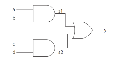
y = s1 + s2; where s1=ab and s2 =cd The Boolean function of y could be written as: Y = ab + cd VHDL Description: library IEEE; use IEEE.STD_LOGIC_1164.ALL; entity andor is port (a,b,c,d: in std_logic; y : out std_logic); end andor; architecture andor_dtfl of andor is signal s1,s2 : std_logic; begin s1 <= a and b; --statement 1. S2 <= c and d; --statement 2. Y <= s1 or s2; --statement 3. End andor_dtfl;
Verilog description: module andor (a,b,c,d, y ); input a,b,c,d; output y; wire s1, s2; / wire statement here is not necessarily needed since s1 and s2 are single bit/ assign s1 = a & b; //statement 1. assign s2 = c & d; //statement 2. assign y = s1 | s2; //statement 3. |
|
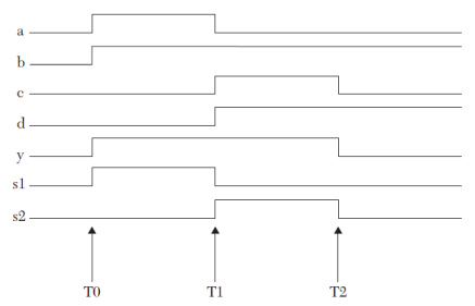
Simulation waveform
From above examples, the input and output signals are declared in the entity (module) as ports. In HDL, a signal has to be declared before it can be used.
Accordingly, signals s1 and s2 have to be declared. In VHDL, s1 and s2 are declared as signals by using the predefined word signal in the architecture:
signal s1, s2 : bit;
In Verilog, s1 and s2 are declared as signals by using the predefined word wire:
wire s1, s2;
By default, all ports in Verilog are assumed to be wires. The value of the wire is continuously changing with changes in the device that is deriving it.
A signal-assignment statement is used to assign a value to a signal. The left-hand side of the statement should be declared as a signal. The right-hand side can be a signal, a variable, or a constant. The operator for signal assignment is <= in VHDL or the predefined word assign in Verilog.
Signal-assignment statement in HDL gets executed only when an event occur on its right-hand side. If no event occurred on any statement, this statement would not be executed. An event is a change in the value of a signal or variable such as a change from 0 to 1 (from low to high) or from 1 to 0 (from high to low). The statement that receives an event first will be executed first regardless of the order of its placement in the HDL code.
The signal-assignment statement is executed in two phases: calculation and assignment. If an event occurs on the right-hand side of a statement, then this side is calculated at the time of the event; after calculation, the value obtained from the calculation is assigned to the left-hand side, taking into consideration any timing information given in the statement
A constant in HDL is treated as it is in C language; its value is constant within the segment of the program where it is visible. A constant in VHDL can be declared using the predefined word constant. In Verilog, a constant can be declared by its type such as time or integer. For example, the following statements declare period as a constant of type time:
constant period : time; -- VHDL
time period; // Verilog
To assign a value to a constant, use the assignment operator := in VHDL or = in Verilog. For example, to assign a value of 100 nanoseconds to the constant period described above:
period := 100 ns; -- VHDL
period = 100; // Verilog
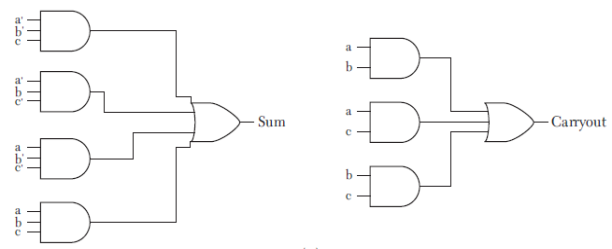
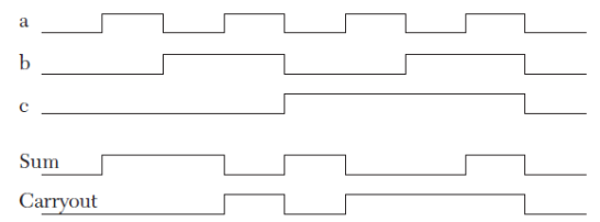
A full adder is a combinational circuit that adds three input bits (a + b + c) and outputs the result as two bits; one bit for the sum and one bit for the carryout.
Truth table
The logic diagram can be drawn as:
HDL code for full adder: VHDL description: library IEEE; use IEEE.STD_LOGIC_1164.ALL; entity fulladder is Port ( a,b,c : in std_logic; sum, Carryout : out std_logic); end fulladder; architecture flad_dtfl of fulladder is begin Sum <= (not a and not b and c) or (not a and b and not c) or (a and not b and not c) or (a and b and c); Carryout <= (a and b) or (a and c) or (b and c); end flad_dtfl; Verilog description: module fulladder(a, b, c); output Sum, Carryout; input a, b, c; assign Sum = (~ a & ~ b & c)|( ~ a & b & ~c)| ( a & ~b & ~c)|( a & b & c) ; assign Carryout = (a & b) | (a & c) | (b & c); endmodule
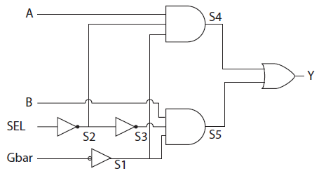
2. 2*1 Multiplexer A 2x1 multiplexer is a combinational circuit; it has two one-bit inputs, a one-bit select line, and a one-bit output. Additional control signals may be added, such as enable. The output of the basic multiplexer depends on the level of the select line. If the select is high (1), the output is equal to one of the two inputs. If the select is low (0), the output is equal to the other input.
If the enable (Gbar) is high (1), the output is low (0) regardless of the input. When Gbar is low (0), the output is A if SEL is low (0), or the output is B if SEL is high (1). The Boolean function of the output Y is: Y = (S1 and A and SEL) or (S1 and B and SEL); S1 is the invert of Gbar.
HDL Code of a 2x1 Multiplexer:
VHDL description:
library IEEE; use IEEE.STD_LOGIC_1164.ALL; entity mux2x1 is port (A, B, SEL, Gbar : in std_logic; Y : out std_logic); end mux2x1; architecture MUX_DF of mux2x1 is signal S1, S2, S3, S4, S5 : std_logic; constant dly : time := 7ns; Begin -- Assume 7 nanoseconds propagation delay -- for all and, or, and not operation. st1: Y <= S4 or S5 after dly; st2: S4 <= A and S2 and S1 after dly; st3: S5 <= B and S3 and S1 after dly; st4: S2 <= not SEL after dly; st5: S3 <= not S2 after dly; st6: S1 <= not Gbar after dly; end MUX_DF;
Verilog Description:
module mux2x1 (A, B, SEL, Gbar, Y); input A, B, SEL, Gbar; output Y; wire S1, S2, S3, S4, S5; time dly = 7; /*Assume 7 time units delay for all and, or, not operations. The delay here is expressedin simulation screen units. */ assign # dly Y = S4 | S5; //st1 assign #dly S4 = A & S2 & S1; //st2 assign #dly S5 = B & S3 & S1; //st3 assign #dly S2 = ~ SEL; //st4 assign #dly S3 = ~ S2; //st5 assign #dly S1 = ~ Gbar; //st6 endmodule
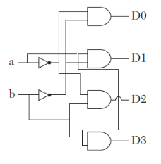
3. 2*4 Decoder A decoder is a combinational circuit. A 2x4 decoder has two inputs and four outputs. For any input, only one output is active; all others are inactive. For active high output decoders, only one output is high. The output of n-bit input decoder is 2n bits.
The Boolean function of the outputs can be written as: D0 = a’ b’ D1 = a b’ D2 = a’ b D3 = a b
HDL Code of a 2x4 Decoder without Time Delay
VHDL description:
library IEEE; use IEEE.STD_LOGIC_1164.ALL; entity decoder2x4 is port ( a, b : in std_logic; D : out std_logic_vector (3 downto 0)); end decoder2x4; architecture decder_dtfl of decoder2x4 is begin D(0) <= not a and not b; D(1) <= a and not b; D(2) <= not a and b; D(3) <= a and b; end decder_dtfl;
Verilog description:
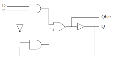
module decoder2x4( a, b, D); input a,b; output [3:0]D; assign D[0] = ~a & ~ b; assign D[1] = a & ~ b; assign D[2] = ~a & b; assign D[3] = a & b; endmodule 4. D-Latch Latches are sequential circuits. The output of a sequential circuit depends on the current state and the input. At any time (T) the present value of Q is called the current state. At any selected time (T + ts) the value of Q is called the next state Q+. The value of the next state depends on the value of the present state and the value of the input
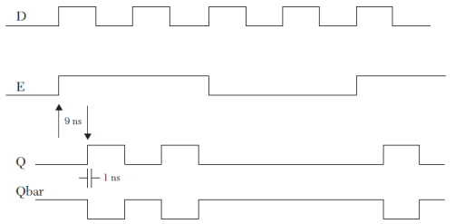
Qbar (Qbar+) is always the inverse of Q (Q+). To find the Boolean function, use K-maps to minimize the minterms.
Q = E’Q + ED Qbar = Q’
HDL Code for a D-Latch: VHDL and Verilog
VHDL Description:
library IEEE; use IEEE.STD_LOGIC_1164.ALL; entity D_Latch is port (D, E : in std_logic; Q, Qbar : buffer std_logic); --Q and Qbar are declared as buffer because they act --as both input and output, they appear on the --right and left hand side of a signal assignment. --inout or linkage could have been used instead of buffer. end D_Latch; architecture DL_DtFl of D_Latch is constant Delay_EorD : Time := 9 ns; constant Delay_inv : Time := 1 ns; begin --Assume 9-ns propagation delay time between --E or D and Qbar; and 1 ns between Qbar and Q. Qbar <= (D and E) nor (not E and Q) after Delay_EorD; Q <= not Qbar after Delay_inv; end DL_DtFl;
Verilog Description:
module D_latch (D, E, Q, Qbar); input D, E; output Q, Qbar; time Delay_EorD = 9; time Delay_inv = 1; assign #Delay_EorD Qbar = ~((E & D) | (~E & Q)); assign #Delay_inv Q = ~ Qbar; endmodule
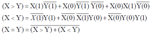
5. 2 bit Comparator A two-bit comparator is a combinational circuit that compares two words (numbers); each word has two bits. Let the two words be X and Y. The output of the comparator indicates the result of the comparison: X > Y, X = Y, or X < Y. Because the number of input bits is small (a total of four input bits), a truth table of the comparator can be used to find the Boolean function.
The Boolean expression using K map can be found as:
HDL Code of a 2x2 Magnitude Comparator
VHDL Description:
library IEEE; use IEEE.STD_LOGIC_1164.ALL; entity COMPR_2 is port (x, y : in std_logic_vector(1 downto 0); xgty, xlty : buffer std_logic; xeqy : out std_logic); end COMPR_2; architecture COMPR_DFL of COMPR_2 is begin xgty <= (x(1) and not y(1)) or (x(0) and not y(1) and not y(0)) or x(0) and x(1) and not y(0)); xlty <= (y(1) and not x(1)) or ( not x(0) and y(0) and y(1)) or (not x(0) and not x(1) and y(0)); xeqy <= xgty nor xlty; end COMPR_DFL;
Verilog Description:
input [1:0] x, y; output xgty, xlty, xeqy; assign xgty = (x[1] & ~ y[1]) | (x[0] & ~ y[1] & ~ y[0]) | (x[0] & x[1] & ~ y[0]); assign xlty = (y[1] & ~ x[1] ) | (~ x[0] & y[0] & y[1]) |(~ x[0] & ~ x[1] & y[0]); assign xeqy = ~ (xgty | xlty); endmodule | |||||||||||||||||||||||||||||||||||||||||||||||||||||||||||||||||||||||||||||||||||||||||||||||||||||||||||||||||||||||||||||||||||||||||||||||||||||||||||||||||||||||||||||||||||||||||||||||||||||||||||||||||||||||||||||||||||||||||||||||||||||||||||||||||||
A vector is a data type that declares an array of similar elements, such as declaring an object that has a width of more than one bit. In the previous examples, all signals have been one-bit in width. If signal A has a four-bit width, it can be declared as four different signals, a0, a1, a2, a3, as shown:
signal a0, a1, a2, a3 : bit; -- VHDL wire a0, a1, a2, a3; // Verilog
Or, it can be declared using the vector declaration:
signal a : bit_vector (3 downto 0); -- VHDL wire [3:0] a; // Verilog
In VHDL, downto ([3:0 ] in Verilog) is a predefined operator that describes the width of the vector. If the value of a is 14d, or (1110)2, then the elements of vector (array) a are: a(3) = 1 a(2) = 1 a(1) = 1 a(0) = 0 The following declaration can also be used:
signal a : bit_vector (0 to 3); -- VHDL wire [0:3] a; // Verilog
where to is a predefined word. In the above declaration, the elements of the vector are: a(0) = 1 a(1) = 1 a(2) = 1 a(3) = 0
This means the value of a is considered to be 7d rather than 14d. |
- HDL Programming (VHDL and Verilog)- Nazeih M.Botros- John Weily India Pvt. Ltd. 2008.
- Fundamentals of HDL – Cyril P.R. Pearson/Sanguin 2010.
- VHDL -Douglas perry-Tata McGraw-Hill
- A Verilog HDL Primer- J.Bhaskar – BS Publications
- Circuit Design with VHDL-Volnei A.Pedroni-PHI


