UNIT-4
Structural Descriptions
Structural description is best achieved when the digital logic of the details of hardware components of the system are well-known.
For eg- A 2*1 multiplexer consist of AND, OR and NOT gates. Structural description can easily illustrate these components.
Structural description is very close to schematic simulation. Following are some of the points regarding structural description:
- Structural description simulates the system by describing its logical components. The components can be gate level or a higher logical level, such as register-transfer level (RTL).
- It is more convenient to use structural description than behavioral description for systems that require specific design constraints.
- All statements in structural description are concurrent. At any simulation time, all statements that have an event are executed concurrently.
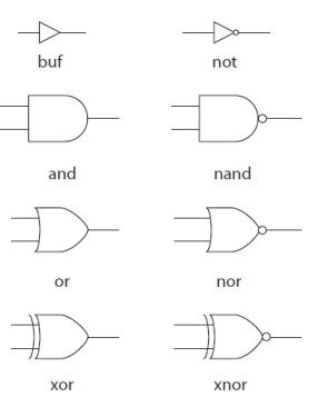
- A major difference between VHDL and Verilog structural description is the availability of components (especially primitive gates) to the user. Verilog recognizes all the primitive gates such as AND, OR, XOR, NOT, and XNOR gates. Basic VHDL packages do not recognize any gates unless the package is linked to one or more libraries, packages, or modules that have the gate description.
Let us take an example of Halfadder. VHDL Description --This code is not complete; binding statements should --be added to recognize components library IEEE; use IEEE.STD_LOGIC_1164.ALL; entity system is port (a, b : in std_logic; sum, cout : out std_logic); end system; architecture struct_exple of system is --start declaring all different types of components component xor2 port (I1, I2 : in std_logic; O1 : out std_logic); end component; component and2 port (I1, I2 : in std_logic; O1 : out std_logic); end component; begin --Start of instantiation statements X1 : xor2 port map (a, b, sum); A1 : and2 port map (a, b, cout); end struct_exple; Verilog Description module system (a, b, sum, cout); input a, b; output sum, cout; xor X1 (sum, a, b); /* X1 is an optional identifier; it can be omitted.*/ and a1 (cout, a, b); /* a1 is optional identifier; it can be omitted.*/ Endmodule The entity (VHDL) or module (Verilog) name is system; there are two inputs, a and b, and two outputs, sum and cout. The entity or module declaration is the same as in other description styles previously covered (data flow and behavioral). In the VHDL description, the structural code (inside the architecture) has two parts: declaration and instantiation. In declaration, all of the different types of components are declared. For example, the statements component xor2 port (I1, I2 : in std_logic; O1 : out std_logic); end component; declare a generic component by the name of xor2; the component has two inputs (I1, I2) and one output (O1). The name (identifier) xor2 is not a reserved or predefined word in VHDL; it is a user-selected name. To specify the type of the component, additional information should be given to the simulator (see Listing 4.2). If the system has two or more identical components, only one declaration is needed. The instantiation part of the code maps the generic inputs/outputs to the actual inputs/outputs of the system. For example, the statement X1 : xor2 port map (a, b, sum); maps input a to input I1 of xor2, input b to input I2 of xor2, and output sum to output O1 of xor2. This mapping means that the logic relationship between a, b, and sum is the same as between I1, I2, and O1. If xor2 is specified through additional statements to be a XOR gate, for example, then sum = a xor b. A particular order of mapping can be specified as: X1 : xor2 port map (O1 => S, I1 => b , I2 => a); S is mapped to O1, b is mapped to I1, and a is mapped to I2. Note that the mapping of S is written before writing the mapping of the inputs; we could have used any other order of mapping. As previously mentioned, structural description statements are concurrent and are driven by events. This means that their execution depends on events, not on the order in which the statements are placed in the module. So, placing statement A1 before statement X1 does not change the outcome of the VHDL program. Verilog has a large number of built-in gates. For example, the statement: xor X1 (sum, a, b); describes a two-input XOR gate. The inputs are a and b, and the output is sum. X1 is an optional identifier for the gate; the identifier can be omitted as: xor (sum, a, b);
Verilog built-in gate
HDL Code of Half Adder: VHDL and Verilog VHDL Description library IEEE; use IEEE.STD_LOGIC_1164.ALL; entity xor2 is port(I1, I2 : in std_logic; O1 : out std_logic); end xor2; architecture Xor2_0 of xor2 is begin O1 <= I1 xor I2; end Xor2_0; library IEEE; use IEEE.STD_LOGIC_1164.ALL; entity and2 is port (I1, I2 : in std_logic; O1 : out std_logic); end and2; architecture and2_0 of and2 is begin O1 <= I1 and I2; end and2_0; library IEEE; use IEEE.STD_LOGIC_1164.ALL; entity half_add is port (a, b : in std_logic; S, C : out std_logic); end half_add; architecture HA_str of half_add is component xor2 port (I1, I2 : in std_logic; O1 : out std_logic); end component; component and2 port (I1, I2 : in std_logic; O1 : out std_logic); end component; begin X1 : xor2 port map (a, b, S); A1 : and2 port map (a, b, C); end HA_str; Verilog Description: Module system (a, b, sum, cout); input a, b; output sum, cout; xor X1 (sum, a, b); endmodule |
Binding in HDL is common practice. Binding (linking) segment1 in HDL code to segment2 makes all information in segment2 visible to segment1. Example: Binding Between Entity and Architecture in VHDL entity one is port (I1, I2 : in std_logic; O1 : out std_logic); end one; architecture A of one is signal s : std_logic; .......... end A; architecture B of one is signal x : std_logic; ....... end B; Architecture A is bound to entity one through the predefined word of. Also, architecture B is bound to entity one through the predefined word of. Accordingly, I1, I2, and O1 can be used in both architecture A and architecture B. Architecture A is not bound to architecture B, so signal s is not recognized in architecture B. Likewise, signal x is not recognized in architecture A.
Binding Between Entity and Component in VHDL entity orgate is port (I1, I2 : in std_logic; O1 : out std_logic); end orgate; architecture Or_dataflow of orgate is begin O1 <= I1 or I2; end Or_dataflow; entity system is port (x, y, z : in std_logic; out r : std_logic_vector (3 downto 0); end system; architecture system_str of system is component orgate port (I1, I2 : in std_logic; O1 : std_logic); end component; begin orgate port map (x, y, r(0)); ....... end system_str; The component orgate is bound to the entity orgate because it has the same name. Architecture Or_dataflow is bound to entity orgate by the word of. All information in the entity is now visible to the component. Accordingly, the relationship between I1, I2, and O1 defined in the architecture or_dataflow is visible to the component orgate; hence, the component orgate is an OR gate. Now consider another way of VHDL binding where a library or a package is bound to a module. Binding Between Library and Module in VHDL library IEEE; use IEEE.STD_LOGIC_1164.ALL; entity system is port (I1, I2 : in std_logic; O1 : out std_logic_vector (3 downto 0)); end system; architecture lib_bound of system is signal s : std_logic; ............. end lib_bound; IEEE is the name of the library, library and use are a predefined words, and IEEE.STD_LOGIC_1164.ALL refers to the part of the library to be linked. Library IEEE gives the definition for the standard_logic type. By entering the name of the library and the statement use, all information in the library is visible to the module. If the first two statements are absent, the standard_logic type cannot be identified. Libraries can also be created by the user. The HDL simulator creates a library named work every time it compiles code. This library can be bound to another module by using the statement use, as follows: use entity work.gates (or_gates);
Binding Between a Library and Component in VHDL --First, write the code that will be bound to another -- module library IEEE; use IEEE.STD_LOGIC_1164.ALL; entity bind2 is port (I1, I2 : in std_logic; O1 : out std_logic); end bind2; architecture xor2_0 of bind2 is begin O1 <= I1 xor I2; end xor2_0; architecture and2_0 of bind2 is begin O1 <= I1 and I2; end and2_0; architecture and2_4 of bind2 is begin O1 <= I1 and I2 after 4 ns; end and2_4; --After writing the above code; compile it and store it -- in a known location. Now, open another module --where the above information is to be used. library IEEE; use IEEE.STD_LOGIC_1164.ALL; entity half_add is port (a, b : in std_logic; S, C : out std_logic); end half_add; architecture HA_str of half_add is component xor2 port (I1, I2 : in std_logic; O1 : out std_logic); end component; component and2 port (I1, I2 : in std_logic; O1 : out std_logic); end component; for all : xor2 use entity work.bind2 (xor2_0); for all : and2 use entity work.bind2 (and2_4); begin X1 : xor2 port map (a, b, S); A1 : and2 port map (a, b, C); end HA_str; The statement for all : xor2 use entity work.bind2 (xor2_0) binds the architecture xor2_0 of the entity bind2 to the component xor2. By this binding, component xor2 behaves as a two-input XOR gate with zero propagation delay. The statement for all : and2 use entity work.bind2 (and2_4) binds the architecture and2_4 of the entity bind2 to the component and2. By this binding, component and2 behaves as a two-input AND gate with a 4-ns propagation delay.
Binding Between Two Modules in Verilog module one (O1, O2, a, b); input [1:0] a; input [1:0] b; output [1:0] O1, O2; two M0 (O1[0], O2[0], a[0], b[0]); two M1 (O1[1], O2[1], a[1], b[1]); endmodule module two (s1, s2, a1, b1); input a1; input b1; output s1, s2; xor (s1, a1, b1); and (s2, a1, b1); endmodule The statement: two M0 (O1[0], O2[0], a[0], b[0]); written in module one binds module two to module one. O1[0] is the output of a two-input XOR gate with a[0] and b[0] as the inputs O2[1] is the output of a two-input AND gate with a[1] and b[1] as the inputs Examples of Binding in Structural Descriptions:
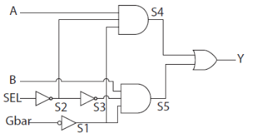
VHDL Description library IEEE; use IEEE.STD_LOGIC_1164.ALL; entity mux2x1 is port (A, B, SEL, Gbar : in std_logic; Y : out std_logic); end mux2x1; architecture mux_str of mux2x1 is --Start components Declaration component and3 port (I1, I2, I3 : in std_logic; O1 : out std_logic); end component; --Only different types of components need be declared. --Since the multiplexer has two identical AND gates, --only one is declared. component or2 port (I1, I2 : in std_logic; O1 : out std_logic); end component; component Inv port (I1 : in std_logic; O1 : out std_logic); end component; signal S1, S2, S3, S4, S5 : std_logic; for all : and3 use entity work.bind3 (and3_7); for all : Inv use entity work.bind1 (inv_7); for Or1 : or2 use entity work.bind2 (or2_7); begin --Start instantiation A1 : and3 port map (A,S2, S1, S4); A2 : and3 port map (B,S3, S1, S5); IV1 : Inv port map (SEL, S2); IV2 : Inv port map (Gbar, S1); IV3 : Inv port map (S2, S3); or1 : or2 port map (S4, S5, Y); end mux_str;
Verilog Description module mux2x1 (A, B, SEL, Gbar, Y); input A, B, SEL, Gbar; output Y; and #7 (S4, A, S2, S1); or #7 (Y, S4, S5); and #7 (S5, B, S3, S1); not #7 (S2, SEL); not #7 (S3, S2); not #7 (S1, Gbar); endmodule
2. VHDL Behavioral Description of a Tri-State Buffer
entity bind2 is port (I1, I2 : in std_logic; O1 : out std_logic); end bind2; ........... --Add the following architecture to --the entity bind2 of Listing 4.8 architecture bufif1 of bind2 is begin buf : process (I1, I2) variable tem : std_logic; begin if (I2 =’1’) then tem := I1; else tem := ‘Z’; end if; O1 <= tem; end process buf; end bufif1;
3. HDL Description of a 2x4 Decoder with Tri-State Output VHDL Description library IEEE; use IEEE.STD_LOGIC_1164.ALL; entity decoder2x4 is port (I : in std_logic_vector(1 downto 0); Enable : in std_logic; D : out std_logic_vector (3 downto 0)); end decoder2x4; architecture decoder of decoder2x4 is component bufif1 port (I1, I2 : in std_logic; O1 : out std_logic); end component; component inv port (I1 : in std_logic; O1 : out std_logic); end component; component and2 port (I1, I2 : in std_logic; O1 : out std_logic); end component; for all : bufif1 use entity work.bind2 (bufif1); for all : inv use entity work.bind1 (inv_0); for all : and2 use entity work.bind2 (and2_0); signal s0, s1, s2, s3 : std_logic; signal Ibar : std_logic_vector (1 downto 0); -- The above signals have to be declared before they -- can be used begin B0 : bufif1 port map (s0, Enable, D(0)); B1 : bufif1 port map (s1, Enable, D(1)); B2 : bufif1 port map (s2, Enable, D(2)); B3 : bufif1 port map (s3, Enable, D(3)); iv0 : inv port map (I(0), Ibar(0)); iv1 : inv port map (I(1), Ibar(1)); a0 : and2 port map (Ibar(0), Ibar(1), s0); a1 : and2 port map (I(0), Ibar(1), s1); a2 : and2 port map (Ibar(0), I(1), s2); a3 : and2 port map (I(0), I(1), s3); end decoder;
Verilog Description module decoder2x4 (I, Enable, D); input [1:0] I; input Enable; output [3:0] D; wire [1:0] Ibar; bufif1 (D[0], s0, Enable); bufif1 (D[1], s1, Enable); bufif1 (D[2], s2, Enable); bufif1 (D[3], s3, Enable); not (Ibar[0], I[0]); not (Ibar[1], I[1]); and (s0, Ibar[0], Ibar[1]); and (s1, I[0], Ibar[1]); and (s2, Ibar[0], I[1]); and (s3, I[0], I[1]); endmodule
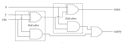
4. Structural description of a full adder
VHDL Description
library IEEE; use IEEE.STD_LOGIC_1164.ALL; entity bind22 is Port (I1, I2 : in std_logic; O1, O2 : out std_logic); end bind22; architecture HA of bind22 is component xor2 port (I1, I2 : in std_logic; O1 : out std_logic); end component; component and2 port (I1, I2 : in std_logic; O1 : out std_logic); end component; VHDL Description library IEEE; use IEEE.STD_LOGIC_1164.ALL; entity FULL_ADDER is Port (x, y, cin : in std_logic; sum, carry : out std_logic); end FULL_ADDER; architecture full_add of FULL_ADDER is component HA Port (I1, I2 : in std_logic; O1, O2 : out std_logic); end component; component or2 Port (I1, I2 : in std_logic; O1 : out std_logic); end component; for all : HA use entity work.bind22 (HA); for all : or2 use entity work.bind2 (or2_0); signal s0, c0, c1 : std_logic; begin HA1 : HA port map (y, cin, s0, c0); HA2 : HA port map (x, s0, sum, c1); r1 : or2 port map (c0, c1, carry); end full_add; Verilog Description module FULL_ADDER (x, y, cin, sum, carry); input x, y, cin; output sum, carry; HA H1 (y, cin, s0, c0); HA H2 (x, s0, sum, c1); //The above two statements bind module HA //to the present module FULL_ADDER or (carry, c0, c1); endmodule module HA (a, b, s, c); input a, b; output s, c; xor (s, a, b); and (c, a, b); endmodule 5. Structural description of an set-reset latch
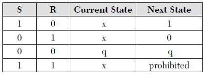
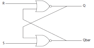
VHDL Description library IEEE; use IEEE.STD_LOGIC_1164.ALL; entity SR_latch is port (R, S : in std_logic; Q, Qbar : buffer std_logic); --Q, Qbar are declared buffer because --they behave as input and output. end SR_latch; architecture SR_strc of SR_latch is --Some simulators would not allow mapping between --buffer and out. In this --case, change all out to buffer. component nor2 port (I1, I2 : in std_logic; O1 : out std_logic); end component; for all : nor2 use entity work.bind2 (nor2_0); begin n1 : nor2 port map (S, Q, Qbar); n2 : nor2 port map (R, Qbar, Q); end SR_strc;
Verilog Description module SR_Latch (R, S, Q, Qbar); input R, S; output Q, Qbar; nor (Qbar, S,Q); nor (Q, R, Qbar); endmodule
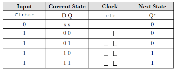
6. Structural description of a pulse-triggered, Master-slave d flip-flop with active low clear
VHDL Description
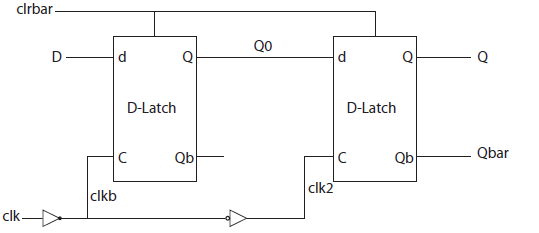
library IEEE; use IEEE.STD_LOGIC_1164.ALL; entity D_FFMasterWclr is Port (D, clk, clrbar : in std_logic; Q, Qbar : buffer std_logic); end D_FFMasterWclr ; architecture D_FF_str of D_FFMasterWclr is component inv port (I1 : in std_logic; O1 : buffer std_logic); end component; component D_latchWclrbar port (I1, I2, I3 : in std_logic; O1, O2 : buffer std_logic); end component; for all : D_latchWclrbar use entity work. bind32(D_latch_Wclr); for all : inv use entity work.bind1 (inv_1); signal clkb, clk2, Q0, Qb0 : std_logic; begin D0 : D_latchWclrbar port map (D, clkb,clrbar, Q0, Qb0); D1 : D_latchWclrbar port map (Q0, clk2, clrbar, Q, Qbar); in1 : inv port map (clk, clkb); in2 : inv port map (clkb, clk2); end D_FF_str;
Verilog Description module D_FFMasterWclr(D, clk,clrbar, Q, Qbar); input D, clk, clrbar; output Q, Qbar; not #1 (clkb, clk); not #1 (clk2, clkb); D_latchWclr D0 (D, clkb,clrbar, Q0, Qb0); D_latchWclr D1 (Q0, clk2,clrbar, Q, Qbar); endmodule
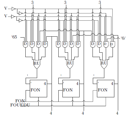
7. Structural description of a three-bit universal Shift register
Verilog Description of a Three-Bit Universal Shift Register module shft_regsterUniv(clk, clrbar, s0,s1,P,DSR,DSL,Q,Qb); input clk, clrbar,s0,s1,DSR,DSL; output [2:0] Q,Qb,P; not (s0bar, s0); not (s0t,s0bar); not (s1bar, s1); not (s1t, s1bar); and #4 a0(aa0, DSR, s1bar,s0t); and #4 a1(aa1, s0t, s1t,P[2]); and #4 a2(aa2, s0bar, s1t,Q[1]); and #4 a3(aa3, s0bar, s1bar,Q[2]); or #4 or2 (D2,aa0,aa1,aa2,aa3); D_FFMasterWclr DFM0(D2,clk,clrbar,Q[2],Qb[2]); and #4 a4(aa4, Q[2], s1bar,s0t); and #4 a5(aa5, s0t, s1t,P[1]); and #4 a6(aa6, s0bar, s1t,Q[0]); and #4 a7(aa7, s0bar, s1bar,Q[1]); or #4 or1 (D1,aa4,aa5,aa6,aa7); D_FFMasterWclr DFM1(D1,clk, clrbar,Q[1],Qb[1]); and #4 a8(aa8, Q[1], s1bar,s0t); and #4 a9(aa9, s0t, s1t,P[0]); and #4 a10(aa10, s0bar, s1t,DSL); and #4 a11(aa11, s0bar, s1bar,Q[0]); or #4 or0 (D0,aa8,aa9,aa10,aa11); D_FFMasterWclr DFM2(D0,clk,clrbar,Q[0], Qb[0]); Endmodule |
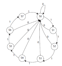
Synchronous sequential circuits are called state machines. The main components of the state machine are latches and flip-flops; and combinational components may also be present. Synchronous clock pulses are fed to all flip-flops and latches of the machine. There are two types of synchronous sequential circuits:
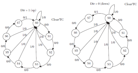
The output or next state of Mealy circuits depends on the inputs and the present (current) state of the flip-flops/latches. The output or next state of the Moore circuit depends only on the present states. The current state is the value of Q just before the present clock pulse or edge; the next state is the value of Q after the clock pulse or the edge. To build a state machine, the following steps are performed:
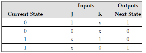
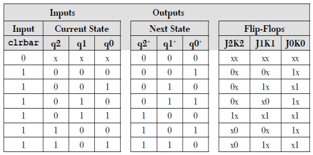
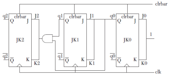
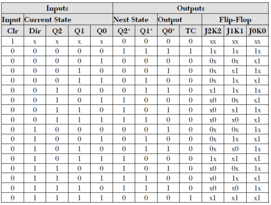
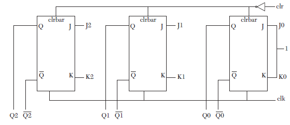
1. Determine the number of states. If the system is n-bit, then the number of flip-flops is n, and the number of states is 2n. 2. Construct a state diagram that shows the transition between states. At each state, consider it as the current state; after the clock is active, the system moves from current state to next state. Determine the next state according to the input if the system is Mealy or according to the current state only if the system is Moore. Also, determine the output (if any) of the system at this current state. 3. From the state diagram, construct the excitation table that tabulates the inputs and the outputs. The inputs always include the current states, and the outputs always include the next states. The table also includes the inputs of the flip-flops or latches that constitute the state machine. 4. Find J and K in terms of the inputs and minimize using K-maps. 5. If using structural description to simulate the system, draw a logic diagram of the system.
Examples of State machine with Structural Description:
Now, construct the K-maps of the Table and find expressions
J0 = K0=1 J1 = K1 = q0 J2 = K2= q0 q1
In VHDL, declare JK FF as component:
component JK_FLFL port (J, K, clk, clrbar : in std_logic; Q, Qbar : buffer std_logic); end component; for all : JK_FLFL use entity work. JK_FLFL (JK_Master);
VHDL Description library IEEE; use IEEE.STD_LOGIC_1164.ALL; entity CTStatemachine is port( clk, clrbar : in std_logic; Q, Qbar: buffer std_logic_vector (2 downto 0)); end CTStateMachine; architecture ct_3 of CTStateMachine is component and2 port (I1, I2 : in std_logic; O1 : buffer std_logic); end component; component JK_FLFL port (J, K, clk, clrbar : in std_logic; Q, Qbar : buffer std_logic); end component; for all : and2 use entity work.bind2 (and2_4); for all : JK_FLFL use entity work. JK_FLFL (JK_Master ); --Be sure to attach the entity-architectures -- shown above signal J2,K2 : std_logic; begin JK0 : JK_FLFL port map (‘1’, ‘1’, clk, clrbar, Q(0), Qbar(0)); JK1 : JK_FLFL port map (q(0), q(0), clk, clrbar, Q(1), Qbar(1)); A1: and2 port map (q(0), q(1), J2); A2: and2 port map (q(0), q(1), K2); JK2 : JK_FLFL port map (J2, K2, clk, clrbar, Q(2), Qbar(2)); end ct_3;
Verilog Description
module CTstatemachine(clk, clrbar, q, qb); input clk, clrbar; output [2:0] q, qb; JK_FF FF0(1’b1, 1’b1, clk, clrbar, q[0], qb[0]); assign J1 = q[0]; / a buffer could have been used here and in all assign statement in this module/ assign K1 = q[0]; JK_FF FF1 (J1, K1, clk, clrbar, q[1], qb[1]); and A1 (J2, q[0], q[1]); assign K2 = J2; JK_FF FF2(J2, K2, clk, clrbar, q[2], qb[2]); endmodule
2. Structural description of a three-bit synchronous Up/down counter with active high clear
VHDL Description library IEEE; use IEEE.STD_LOGIC_1164.ALL; entity up_down is port (clr, Dir, clk : in std_logic; TC : buffer std_logic; Q, Qbar : buffer std_logic_vector (2 downto 0)); end up_down;
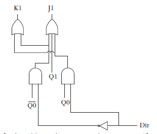
architecture Ctr_updown of up_down is --Some simulators will not allow mapping between --buffer and out. In this --case, change all out to buffer. component inv port (I1 : in std_logic; O1 : buffer std_logic); end component; component and2 port (I1, I2 : in std_logic; O1 : buffer std_logic); end component; component or2 port (I1, I2 : in std_logic; O1 : buffer std_logic); end component; component or3 port (I1, I2,I3 : in std_logic; O1 : buffer std_logic); end component; component and3 port (I1, I2, I3 : in std_logic; O1 : buffer std_logic); end component; component and4 port (I1, I2, I3, I4 : in std_logic; O1 : buffer std_logic); end component; component JK_FLFL port (J, K, clk, clrbar : in std_logic; Q, Qbar : buffer std_logic); end component; for all : JK_FLFL use entity work. JK_FLFL (JK_Master ); for all : inv use entity work.bind1 (inv_1); for all : and2 use entity work.bind2 (and2_4); for all : and3 use entity work.bind3 (and3_4); for all : and4 use entity work.bind4 (and4_4); for all : or2 use entity work.bind2 (or2_4); for all : or3 use entity work.bind3 (or3_4); --Be sure that all the reference entities --above such as JK_FLFL --are attached in the project. signal clrbar, Dirbar, J1, K1, J2, K2 : std_logic; signal s : std_logic_vector (5 downto 0); begin in1 : inv port map (clr, clrbar); in2 : inv port map (Dir, Dirbar); an1 : and2 port map (Dirbar, Qbar(0), s(0)); an2 : and2 port map (Dir, Q(0), s(1)); an3 : and3 port map (Dirbar, Qbar(1), Qbar(0), s(2)); an4 : and3 port map (Dir, Q(1), Q(0), s(3)); an5 : and4 port map (Dir, Q(1), Q(0), Q(2), s(4)); an6 : and4 port map (Dirbar, Qbar(1), Qbar(0), Qbar(2), s(5)); r0 : or3 port map (s(0), s(1), Q(1), J1); r1 : or2 port map (s(0), s(1), K1); r2 : or2 port map (s(2), s(3), J2); K2 <= J2; r3 : or2 port map (s(4), s(5), TC); JKFF0 : JK_FLFL port map (‘1’, ‘1’, clk, clrbar, Q(0), Qbar(0)); JKFF1 : JK_FLFL port map (J1, K1, clk, clrbar, Q(1), Qbar(1)); JKFF2 : JK_FLFL port map (J2, K2, clk, clrbar, Q(2), Qbar(2)); end Ctr_updown;
Verilog Description module up_down(clr, Dir, clk, Q, Qbar, TC); input clr, Dir, clk; output [2:0] Q, Qbar; output TC; not #1 (clrbar, clr); not #1 (Dirbar, Dir); and #4 a1(s0, Dirbar, Qbar[0]); and #4 a2(s1, Dir, Q[0]); and #4 a3(s2, Dirbar, Qbar[0], Qbar[1]); and #4 a4(s3, Q[0], Q[1], Dir); and #4 a5(s4, Dirbar, Qbar[0], Qbar[1], Qbar[2]); and #4 a6(s5, Q[0], Q[1], Q[2],Dir); or #4 r1(J1, s0, Q[1], s1); or #4 r2(K1, s0, s1); or #4 r3(J2, s2, s3); assign K2 = J2;// a buffer can be //used to generate the above statement or #4 r4(TC, s4, s5); JK_FF JKFF0 (1’b1, 1’b1, clk, clrbar, Q[0], Qbar[0]); JK_FF JKFF1 (J1, K1, clk, clrbar, Q[1], Qbar[1]); JK_FF JKFF2 (J2, K2, clk,clrbar, Q[2], Qbar[2]); /Be sure that all the reference entities above such as JK_FLFL are attached in the project./ endmodule
|
The predefined word generate is mainly used for repetition of concurrent statements. Its counterpart in behavioral description is the For-Loop and it can be used to replicate structural or gate-level description statements. In VHDL, the format for the generate statement is: L1 : for i in 0 to N generate v1 : inv port map (Y(i), Yb(i)); --other concurrent statements can be entered here end generate; The above statement describes N + 1 inverters (assuming inv was declared as an inverter component with input Y and output Yb). The input to inverter is Y(i), and the output is Yb(i). L1 is a required label for the generate statement. An equivalent generate statement in Verilog is: generate genvar i; for (i = 0; i <= N; i = i + 1) begin : u not (Yb[i], Y[i]); end endgenerate The statement genvar i declares the index i of the generate statement; genvar is a predefined word. U is a label for the predefined word begin; and begin must have a label. The words generic (in VHDL) and parameter (in Verilog) are used to define global constants. The generic statement can be placed within entity, component, or instantiation statements. The following generic VHDL statement inside the entity declares N as a global constant of value 3: entity compr_genr is generic (N : integer := 3); port (X, Y : in std_logic_vector (N downto 0); xgty, xlty, xeqy : buffer std_logic);
Examples
HDL Description of N-Bit Magnitude Comparator Using the generate Statement: VHDL and Verilog VHDL Description: library IEEE; use IEEE.STD_LOGIC_1164.ALL; entity compr_genr is generic (N : integer := 3); port (X, Y : in std_logic_vector (N downto 0); xgty, xlty, xeqy : buffer std_logic); end compr_genr; architecture cmpare_str of compr_genr is --Some simulators will not allow mapping between --buffer and out. In this --case, change all out to buffer. component full_adder port (I1, I2, I3 : in std_logic; O1, O2 : buffer std_logic); end component; component inv port (I1 : in std_logic; O1 : buffer std_logic); end component; component nor2 port (I1, I2 : in std_logic; O1 : buffer std_logic); end component; component and2 port (I1, I2 : in std_logic; O1 : buffer std_logic); end component; signal sum, Yb : std_logic_vector (N downto 0); signal carry, eq : std_logic_vector (N + 1 downto 0); for all : full_adder use entity work.bind32 (full_add); for all : inv use entity work.bind1 (inv_1); for all : nor2 use entity work.bind2 (nor2_7); for all : and2 use entity work.bind2 (and2_7); begin carry(0) <= ‘0’; eq(0) <= ‘1’; G1 : for i in 0 to N generate v1 : inv port map (Y(i), Yb(i)); FA : full_adder port map (X(i), Yb(i), carry(i), sum(i), carry(i+1)); a1 : and2 port map (eq(i), sum(i), eq(i+1)); end generate G1; xgty <= carry(N+1); xeqy <= eq(N+1); n1 : nor2 port map (xeqy, xgty, xlty); end cmpare_str;
Verilog Description module Compr_genr(X, Y, xgty, xlty, xeqy); parameter N = 3; input [N:0] X, Y; output xgty, xlty, xeqy; wire [N:0] sum, Yb; wire [N+1 : 0] carry, eq; assign carry[0] = 1’b0; assign eq[0] = 1’b1; generate genvar i; for (i = 0; i <= N; i = i + 1) begin : u not (Yb[i], Y[i]); /* The above statement is equivalent to assign Yb = ~Y if outside the generate loop */ FULL_ADDER FA(X[i], Yb[i], carry [i], sum [i], carry[i+1]); /*be sure that the module FULL_ADDER is entered (attached) in the project*/ and (eq[i+1], sum[i], eq[i]); end endgenerate assign xgty = carry[N+1]; assign xeqy = eq[N+1]; nor (xlty, xeqy, xgty); endmodule
2. Structural description of an n-bit asynchronous Down counter using the generate statement
VHDL Description library IEEE; use IEEE.STD_LOGIC_1164.ALL; entity asynch_ctr is Generic (N : integer := 3); -- This is a 3-bit counter. If a different number of -- bits is needed, simply change the -- value of N here only. port (clk, clrbar : in std_logic; Q, Qbar : buffer std_logic_vector (N-1 downto 0)); end asynch_ctr; architecture CT_strgnt of asynch_ctr is --Some simulators will not allow mapping between --buffer and out. In this --case, change all out to buffer. component JK_FLFL port (J, K, clk, clrbar : in std_logic; Q, Qbar : buffer std_logic); end component; for all : JK_FLFL use entity work. JK_FLFL (JK_Master ); -- For bind32, see Listing 4.17a signal h, l : std_logic; signal s : std_logic_vector (N downto 0); begin h <= ‘1’; l <= ‘0’; s <= (Q & clk); -- s is the concatenation of Q and clk. We need -- this concatenation to -- describe the clock of each JK flip-flop. Gnlop : for i in (N-1) downto 0 generate G1 : JK_FLFL port map (h, h, s(i), clrbar, Q(i), Qbar(i)); end generate GnLop; end CT_strgnt;
Verilog Description
module asynch_ctr(clk,clrbar, Q, Qbar); parameter N = 3; /* This is a 3-bit counter. If a different number of bits is needed, simply change the value of N here only.*/ input clk, clrbar; output [N-1:0] Q, Qbar; wire [N:0] s; assign s = {Q, clk}; /*s is the concatenation of Q and clk. This concatenation is needed to describe the clock of each JK flip-flop. */ generate genvar i; for (i = 0; i < N; i = i + 1) begin : u JK_FF JKFF0 (1’b1, 1’b1, s[i],clrbar, Q[i], Qbar[i]); // JK_FF is as shown in Listing 4.17b end endgenerate endmodule |
References:
- HDL Programming (VHDL and Verilog)- Nazeih M.Botros- John Weily India Pvt. Ltd. 2008.
- Fundamentals of HDL – Cyril P.R. Pearson/Sanguin 2010.
- VHDL -Douglas perry-Tata McGraw-Hill
- A Verilog HDL Primer- J.Bhaskar – BS Publications
- Circuit Design with VHDL-Volnei A.Pedroni-PHI
