UNIT-8
Synthesis Basics
Synthesis here means converting HDL behavioral code into logical gates or components which can be downloaded into electronic chips such as field programmable gate arrays (FPGAs).
- Synthesis maps the simulation (software) domain into the hardware domain.
- Synthesis can be viewed as reverse engineering. The user is provided with the behavioral code and is asked to develop the logic diagram.
- Not all HDL statements can be mapped into the hardware domain. The hardware domain is limited to signals that can take zeroes, ones, or are left open. The hardware domain cannot differentiate, for example, between signals and variables, as does the simulation (software) domain.
- To successfully synthesize behavior code into certain electronic chips, the mapping has to conform to the requirements and constraints imposed by the electronic-chip vendor.
- Several synthesis packages are available on the market. These packages can take behavior code, map it, and produce a net list that can be downloaded into the chip.
- Two synthesizers may synthesize the same code using a different number of the same gates. This is due to the different approaches taken by the two synthesizers to map the code.
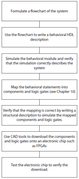
General synthesis steps can be summarized as follows:
Step 1: If the behavioral description is available, go to Step 3. Otherwise, formulate a flowchart for the the system.
Step 2: Use the flowchart to write a behavioral description of the system.
Step 3: Simulate the behavioral code and verify that the simulation correctly
defines the system.
Step 4: Map the behavioral statements into components or logic gates. Be sure that the componentsused are downloadable into the selected chip.
Step 5: Write a structural- or gate-level description of the components and logic gates of Step 4. Simulate the structural description and verify that this simulation is similar to that of Step 3.
Step 6: Use CAD tools to download the gates and components of Step 4 into the electronic chip, usually a FPGA chip.
Step 7: Test the chip by inputting signals to the input pins of the chip and observe the output from the output pins. This step is similar to the verification done in Step 5, except the test here is on real, physical signals.
|
Synthesis Flowchart
Entity (VHDL) or Module in (Verilog) provide information on the inputs and outputs and their types for the system to be synthesized.
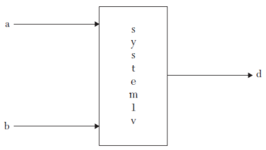
Example-1 - VHDL Code for System1 Entity
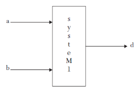
entity system1 is port (a, b : in bit; d : out bit); end system1;
The synthesis information extracted from above example is summarized in the figure below; system1 has two input signals, each one bit, and one output signal of one bit. Each signal can take 0 (low) or 1 (high).
Example-2 - VHDL Code for System3 Entity
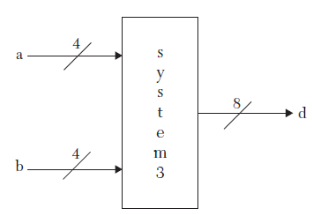
entity system3 is port (a, b : in std_logic_vector (3 downto 0); d : out std_logic_vector (7 downto 0)); end entity system3;
System3 has two four-bit input signals and one eight-bit output signal. The input signals can be binary or left open
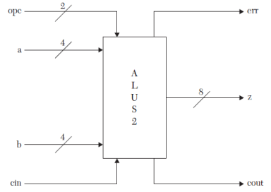
Example-3 - VHDL Code for ALUS2 Entity
VHDL Code for ALUS2 Entity package codes is type op is (add, mul, divide, none); end; use work. codes; entity ALUS2 is port (a, b : in std_logic_vector (3 downto 0); cin : in std_logic; opc : in op; z : out std_logic_vector (7 downto 0); cout : out std_logic; err : out Boolean); end ALUS2;
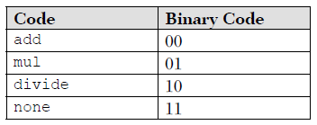
The package codes defines type op. Signal opc is of type op. In our digital hardware domain, there are only zeros and ones. Packages and libraries have no explicit mapping into the hardware domain; they are simulation tools. To map the signal opc into the hardware domain, the signal is decoded. Because the signal can take one of four values (add, mul, divide, or none), it is decoded into two bits.
Example-1- Verilog Code for Module System1v
module system1v (a, b, d); input a, b; output d; endmodule
Module system1v has two input signals, a and b, each of one bit, and one output signal d of one bit. All signals can take 0, 1, or high impedance.
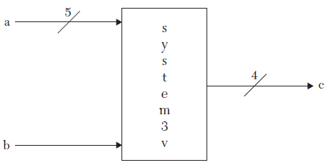
Example-2 Verilog Code for Module System3v module system3v (a, b, c); parameter N = 4; parameter M = 3; input [N:0] a; output [M:0] c; input b; ......... endmodule
|
Process (VHDL) and Always (Verilog) are the major behavioral statements. These statements are frequently used to model systems with data storage such as counters, registers, and CPUs.
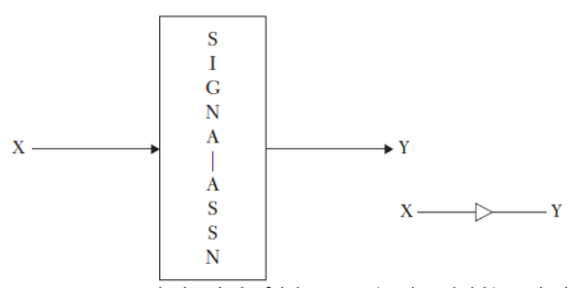
Example-1
Mapping VHDL Code for Signal-Assignment Statement Y <= X
library ieee; use ieee.std_logic_1164.all; entity SIGNA_ASSN is port (X : in bit; Y : out bit); end SIGNA_ASSN; architecture BEHAVIOR of SIGNA_ASSN is begin P1 : process (X) begin Y <= X; end process P1; end BEHAVIOR;
Example-2
Mapping Verilog Code for Signal-Assignment Statement Y = X
module SIGNA_ASSN (X, Y); input X; output Y; reg y; always @ (X) begin Y = X; end endmodule
The variable-assignment statement is a VHDL statement. Verilog does not distinguish between signal- and variable-assignment statements
Example-1
VHDL Variable-Assignment Statement
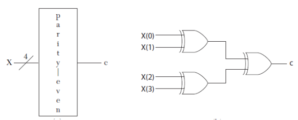
library ieee; use ieee.std_logic_1164.all; entity parity_even is port (x : in std_logic_vector (3 downto 0); C : out std_logic); end parity_even; architecture behav_prti of parity_even is begin P1 : process (x)
variable c1 : std_logic; begin c1 := (x(0) xor x(1)) xor (x(2) xor x(3)); C <= c1; end process P1; end behav_prti;
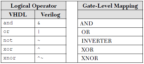
Mapping logical operators is relatively straightforward because finding the gate counterpart of a logical operator is very easy. For example, the mapping of logical operator and (VHDL) or & (Verilog) is an AND gate.
Example: Mapping Logical Operators: VHDL and Verilog
VHDL: Mapping Logical Operators
library IEEE; use IEEE.STD_LOGIC_1164.ALL; entity decod_var is port (a : in std_logic_vector (1 downto 0); D : out std_logic_vector (3 downto 0)); end decod_var; architecture Behavioral of decod_var is begin
dec : process (a) variable a0bar, a1bar : std_logic; begin a0bar := not a(0); a1bar := not a(1); D(0) <= not (a0bar and a1bar); D(1) <= not (a0bar and a(1)); D(2) <= not (a(0) and a1bar); D(3) <= not (a(0) and a(1));
end process dec;
end Behavioral;
Verilog: Mapping Logical Operators
module decod_var (a, D); input [1:0] a; output [3:0] D; reg a0bar, a1bar; reg [3:0] D; always @ (a) begin
a0bar = ~ a[0]; a1bar = ~ a[1];
D[0] = ~ (a0bar & a1bar); D[1] = ~ (a0bar & a[1]); D[2] = ~ (a[0] & a1bar); D[3] = ~ (a[0] & a[1]);
end endmodule
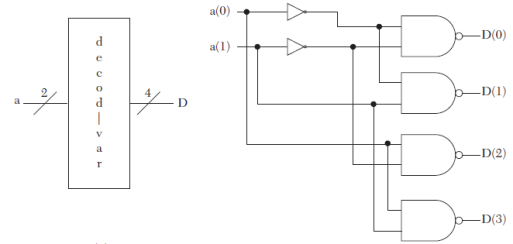
The statements a0bar := not a(0); -- VHDL a0bar = ~ a[0]; // Verilog
represent an inverter. The input to the inverter is the least significant bit of the input a. The statements
D[3] = ~ (a[0] & a[1]); -- VHDL D(3) <= not (a(0) and a(1)); // Verilog
represent a two-input NAND gate. The input is a, and the output is the most significant bit of D.
Example -1 VHDL IF-else Description
process (a, x) begin if (a = '1') then Y <= X; else Y <= '0'; end if; end process;
Verilog IF-else Description
always @ (a, X) begin if (a == 1'b1) Y = X; else Y = 1'b0; end
Its gate level synthesis will be AND gate
Example-2 VHDL Multiplexer IF-else Description
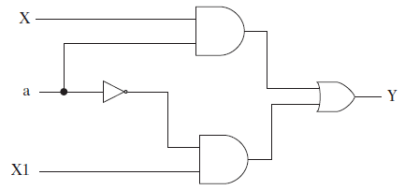
process (a, X, X1) begin if (a = '1') then Y <= X; else Y <= X1; end if; end process;
Verilog Multiplexer IF-else Description
always @ (a, X, X1) begin if (a == 1'b1) Y = X; else Y = X1; end The above IF statement represents a 2x1 multiplexer.
Mapping the case statement is very similar to mapping the IF statement. The case statement is treated as a group of IF statements.
Example -1
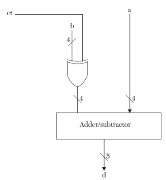
module case_nostr (a, b, ct, d); input [3:0] a, b; input ct; output [4:0] d; reg [4:0] d; always @ (a, b, ct) begin
case (ct) 1’b0 : d = a + b; 1’b1 : d = a - b;
endcase end endmodule
Example-2
case Statement with Storage
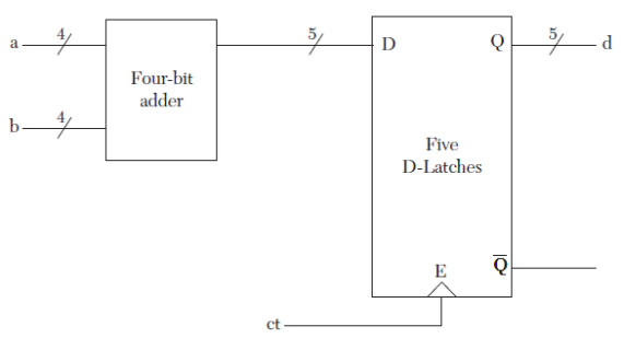
module case_str (a, b, ct, d); input [3:0] a, b; input ct; output [4:0] d; reg [4:0] d; always @ (a, b, ct) begin
case (ct) 1’b0: d = a + b;
1’b1: ; /* This is a blank statement with
no operation (null in VHDL)*/
endcase
end endmodule
Loop in HDL description is an essential tool for behavioral modeling. It is, however, easier to code than it is to synthesize in the hardware domain. The problem is the repetition involved in the loop. Example-1 VHDL For-Loop Statement for i in 0 to 63 loop temp(i) := temp(i) + b(i); end loop; Verilog For-Loop Statement for i = 0; i <= 63; i = i + 1 begin temp[i] = temp[i] + b[i]; end
Each statement is synthesized as a one-bit adder temp(0) = temp(0) + b(0) temp(1) = temp (1) + b(1) temp(2) = temp(2) + b(2) …………………………… temp(63) = temp(63) + b(63)
In the hardware domain, there is no logic for procedures or tasks; they are incorporated in the entity or the module that calls them.
Example-1
A Verilog Example of a Task
module example_task (a1, b1, d1); input a1, b1; output d1; reg d1;
always @ (a1, b1) begin xor_synth (d1, a1, b1); end
task xor_synth; output d; input a, b; begin d = a ^ b; end
endtask endmodule
Example -2
An Example of a Procedure
library IEEE; use IEEE.STD_LOGIC_1164.ALL;
entity Int_Bin is generic (N : integer := 3); port (X_bin : out std_logic_vector (N downto 0); Y_int : in integer; flag_even : out std_logic); end Int_Bin;
architecture convert of Int_Bin is procedure itb (bin : out std_logic_vector; signal flag : out std_logic; N : in integer; int : inout integer) is begin
if (int MOD 2 = 0) then flag <= ‘1’;
else flag <= ‘0’;
end if;
for i in 0 to N loop if (int MOD 2 = 1) then bin (i) := ‘1’; else bin (i) := ‘0’; end if; int := int / 2; end loop;
end itb; begin process (Y_int) variable tem : std_logic_vector (N downto 0); variable tem_int : integer; begin tem_int := Y_int; itb (tem, flag_even, N, tem_int); X_bin <= tem; end process;
end convert;
Example- Verilog Example of a Function
module Func_synth (a1, b1, d1); input a1, b1; output d1; reg d1;
always @ (a1, b1) begin d1 = andopr (a1, b1); end
function andopr; input a, b; begin andopr = a ^ b; end
endfunction endmodule |
In the hardware domain, there is no distinction between the main module and a function; we look to see what the function is performing and then incorporate this information in the entity or module where the function is being called. the function andopr is performing an AND logical operation on two operands.
References:
- HDL Programming (VHDL and Verilog)- Nazeih M.Botros- John Weily India Pvt. Ltd. 2008.
- Fundamentals of HDL – Cyril P.R. Pearson/Sanguin 2010.
- VHDL -Douglas perry-Tata McGraw-Hill
- A Verilog HDL Primer- J.Bhaskar – BS Publications
- Circuit Design with VHDL-Volnei A.Pedroni-PHI
