UNIT 1
Operational Amplifier Fundamentals
|
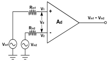
Fig 1 Differential Amplifier
- Vin1 and Vin2 are the two input signals applied at the positive and negative terminals of op-amp.
- Vout is the desired output voltage whose value is equal to the amplified difference between the input voltages.
- Op-amp can amplify both ac and dc voltages hence, the input supply voltages can both be ac or dc.
- Rin1 and Rin2 are source resistances and is negligible w.r.to input resistance Rin.
- Therefore, the voltage drops across them is also assumed to be zero.
- Hence the output voltage,
Vout= Ad (Vin1 - Vin2)
where, Ad is known as open loop gain.
- Hence the output voltage is directly proportional to the product of voltage gain and difference between input voltages.
- The polarity of output voltage depends upon polarity of the difference between input voltages.
Key takeaways
- The output voltage is given as
Vout= Ad (Vin1 - Vin2)
The circuit is designed to have a VCE of 5V across Q2 and Q4. With a ±10 V supply and the bases of Q1 and Q2 at ground level, the voltage drops across R1 and R4 is 5.7 V and 4.3 V respectively. If the input voltage at Q1 base goes down to -4 V, the output terminal and Q2 base also goes down to -4 V as the output follows the input.
This means that the emitter terminals of Q1 and Q2 are pushed down from -0.7 to -4.7 V. Consequently, the collector of Q4 is pushed down by 4 V, reducing VCE4 from 5 V to 1 V. Although Q4 might still be operational with a VCE of 1 V, it is close to saturation. It is seen that there is a limit to the negative going input voltage that can be applied to the op-amp if the circuit is to continue to function correctly.
There is also a limit to positive going input voltages. Where VB1 goes to +4 V, the voltage drop across resistor R1 must be reduced to something less than 1 V, in order to move VB2 and VE3 up by 4 V to follow the input. This requires a reduction in Ic2 to a level that makes Q2 approach cut-off. The input voltage cannot be allowed to become large enough to drive Q2 into cut-off
Output Voltage
The maximum voltage swing is limited by the input voltage range. The output voltage can swing in a positive or negative direction depends on the supply voltage and the op-amp output circuitry. The output voltage should be able to rise until Q5 is near saturation and fall until Q6 approaches saturation.
But because of the circuits that control the output stage, is normally not possible to drive the output transistors close to saturation levels. A rough approximation for most op-amps is that the maximum output voltage swing is approximately equal to 1 V less than the supply voltage. For the 741 op-amp with a supply of ±15 V, the data sheet lists the output voltage swing as typically ±14 V.
Offset voltages
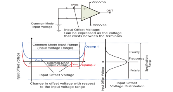
With an input offset voltage and a differential input circuit, ideal op-amps and comparators will have an offset voltage of 0V, including error voltage.
When inputting a common-mode (same) voltage to the input pins of an op-amp or comparator, with an ideal op-amp no output voltage will be output
In case where an input offset voltage exists, a voltage will be output based on the input offset voltage. This input offset voltage, which is the differential voltage required to make the output voltage 0V, becomes the input conversion value.
The Offset voltage is normally expressed in units of mV or µV. Values closer to 0 are more ideal.
|
Fig 4 Op-Amp Parameters
The output offset voltage is the voltage at the output when the differential input voltage is zero.
Offset currents
Bias current compensation will work if both bias currents IB+ and IB- are equal. Since the input transistor cannot be made identical. There will always be some small difference between IB+ and IB-. This difference is called the offset current
|Ios| = IB+-IB------------------------- (7) Offset current Ios for BJT op-amp is 200nA and for FET op-amp is 10pA. Even with bias current compensation, offset current will produce an output voltage when Vi = 0. V1 = IB + R comp And I1 = V1 R1 KCL at node a gives I2 = ( Again V0 = I2 Rf – V1 Vo = I2 Rf - IB+ Rcomp Vo = 1M Ω X 200nA Vo = 200mV with Vi = 0 |
Input and Output Impedance
The input impedance of op-amp is given as
Zif = (1+A Where: A = Gain of op-amp
Zi = Input impedance without feedback The output impedance is given as Zout = Z0/(1+A Zo = output impedance of op-amp |
CMRR
It is the ratio of differential voltage gain Ad to the common mode voltage gain Acm.
CMRR = 
|
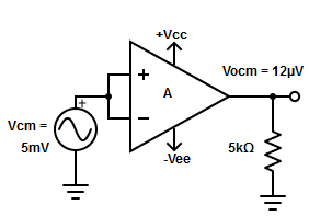
Fig 5 Common Mode Configuration
The common mode voltage gain from above figure can be
 =
= 
Where:
Vocm = output common mode voltage
Vcm = input common mode voltage
Acm = common mode voltage gain
In normal cases the value of Ad is large and Acm is very small making the value of CMRR very high.
Key takeaways
- The common mode voltage gain from above figure can be
 =
= 
PSRR
PSRR = 
 = Change in input offset voltage
 = Change in supply voltage
Slew rate
For example, 1V/us indicates that the voltage can change by 1V in 1us. Ideal op-amps make it possible to faithfully output an output signal for any input signal. However, in reality slew rate limits do exist.
When supplying a rectangular pulse at the input with a steep rise and fall, this indicates the possible degree of change in the output voltage per unit time.
|
Fig 6 Voltage Follower
The rise and fall slew rates are calculated by the following equations:
SRr = ∆ V / ∆ Tr
SRf = ∆ V / ∆ Tf
|
Fig 7 Slew Rate Calculation
Calculate the slew rate
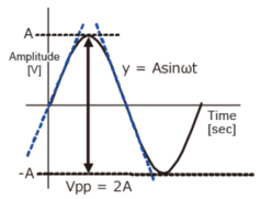
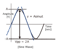
The output is given by y=Asinωt The slew rate is the slope of the tangent of the sine wave, differentiating the above equation.
The slew rate is SR=Aω ω=2πf |
|
Fig 8 Sine wave amplitude
Since the amplitude of the sine wave becomes Vpp=2A (peak-to-peak), the equation can be modified as follows.
|
|
|
|
|
|
|
|
|
This frequency(f) is referred to as the full power bandwidth. These are conditions where the amplification factor in the op-amp has not been set, in other words the relationship of the frequency and amplitude (within the output voltage range) that can be output by the op-amp in a voltage follower circuit.
Key takeaways
- Slew rate is the maximum rate of output voltage change per unit time. It is denoted by S. For getting undistorted output voltage we must have very high slew rate. It is measured in V/sec.
Frequency limitations
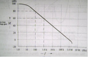
Fig below shows the graph of open loop gain (A) plotted versus frequency (f) for a 741 op-amp. f = 100 Hz, A = 80 dB f = 1 KHz, A = 60 dB
|
Fig 9 Frequency Response
The open loop gain (A) falls by 20 dB when the frequency increases from 100 Hz to 1 KHz. The ten times increase in frequency is termed a decade. So, the rate of the gain is said to be 20 dB per decade. Where internal gain equals to or greater than 80 dB is required for a particular application, it is available with a 741 only for signal frequencies up to ≈100 Hz. A greater than 20 dB is possible for signal frequencies up to ≈ 90 kHz. Other op-amp maintains substantial 1.3 OP-AMP AS DC AMPLIFIERS: Biasing op-amps internal gain to much higher frequencies than the 741
Op-amps must be correctly biased if they are to function properly. The inputs of most op-amps are the base terminals of the transistors in a differential amplifier. transistors to be operational. Base currents must flow into these terminals for the One of the two input terminals is usually connected in some way to the op-amp output to facilitate negative feedback. The other input might be biased directly to ground via a signal source. These amplifiers change their output signal response when experiencing change in its input dc level. A DC amplifier can be inverting, non-inverting or differential.
Key takeaways
- The drawback in using dc amplifiers is that we need to reduce the output offset voltage to zero and this can be achieved by using offset null circuitry.
Av = 1+Rf/R1
|
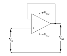
Fig 10 Voltage Follower
In voltage follower feedback resistor is zero because output is directly shorted to input therefore Rf=0
Av = 1
Av = Vo/Vi
Vo=Vi
Non-inverting amplifier
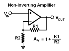
Non- Inverting amplifier is one in which the output is in phase with respect to input that is if you apply a positive voltage, output will be positive. The output is an non -inverted amplified version of input.
|
Fig 11 Non-Inverting Amplifier
Assuming the op-amp is ideal and applying the concept of virtual short, the voltage at the inverting terminal is equal to non- inverting terminal.
Applying KCL at inverting node we get
Vi -Vo/ R2 + Vo – 0 / R1 = 0 By rearranging the terms, we will get
Voltage gain Av = Vo/ Vi = (1+ Rf/Ri)
Gain of non- inverting amplifier Av= (1+ Rf/Ri). |
Design a non-inverting amplifier using Op-amp with a closed loop voltage gain of 10.
Af = 1 + Rf/R1 =10
Rf/R1 = 9
Rf = 9 R1
If R1 = 1K
Rf = 9K Ω
|
Substitute values in above figure. This is the required non-inverting amplifier circuit
Example-2
In an op-amp inverting amplifier R1 = 1K Ω and Rf = 100KΩ. The DC supply voltage of the op-amp is ± 15V. Calculate the output voltage if input voltage is 1V.
R1 = 1KΩ Rf = 100KΩ V+ = 15V and V-=-15V. vi = 1V Af = -Rf/R1 = -100K/1K = -100 Af = vo/vi Vo = Af vi = -100 x 1V = -100V The output voltage cannot exceed the DC power supply voltage . Since vo is negative and large it is limited to V- Vo ≈ V- = -15V |
Inverting Amplifier
Fig 12 Non-Inverting Amplifier
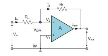
The input signal vi is applied to the inverting input terminal through resistor R1 and non-inverting input terminal is grounded. The feedback from the output of the inverting terminal is provided through the feedback resistor Rf.
Since the input is applied to the inverting terminal vo and vi are opposite in polarity and hence the feedback is negative. Since the non-inverting input terminal is grounded v2=0. Due to virtual short at the input of op-amp the inverting and non-inverting input terminals are at the same potential.
Therefore, v1 = v2 = 0.
Due to high input impedance of Op-amp the current flowing into its inverting input terminal is zero. Therefore, the same current flows through R1 and Rf .
i 1 = i f But i1 = vi – v1 / R1 = vi/R1 i f = v1 – vo / Rf = -vo/Rf vi/R1 = - vo/Rf Af = vo/vi = -Rf/R1 |
Af is the closed loop voltage gain or voltage gain with negative feedback.
Example-1
A 200mV peak to peak sine waveform voltage is applied to Op-amp inverting amplifier with Rf/R1 = 10. Solution Peak to peak input voltage 2Vm = 200 mV Vm = 100 mV Vi= Vm sin wt = 100 sin wt mV Vo = -Rf/R1 x vi = -10 x 100 sinwt mV = -1000 sin wt mV |
Inverting Summing Amplifier
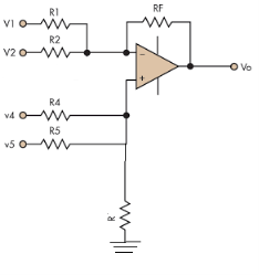
|
Fig13: Summing amplifier
- In the above figure, each terminal is connected with two input sources through resistors. V1 and V2 is connected to the inverting terminal and V4 and V5 is connected to the non-inverting terminal.
- Assuming R1=R2=R4=R5=RF=R.
- Now, on applying superposition theorem, for finding output voltage due to V1 alone, keep V2=V4=V5=0V.
- Hence, now the circuit acts as an inverting amplifier.
- Therefore,
|
- Now, for V4, voltages V1=V2=V5=0V then the circuit behaves as a non-inverting amplifier.


Hence,


Similarly,

So, the resultant output voltage by all the 4 input voltages is given by,
Vo = V01 + V02 + V04 +V05
Vo = -V1 – V2 +V4 + V5
The output voltage Vo is equivalent to the sum all input voltages applied at both the terminals.
In a summing amplifier, if R = 1kΩ, Va = +3V, Vb = +8V, Vc = +9V, Vd = +5V and supply voltage is ±15V. Find the output voltage Vo. Solution: Vo = Sum of all input voltages applied at both the terminals Vo = Va + Vb + Vc +Vd Vo = -3 -8 +9 +5 Vo = +3V |
Example 2:
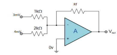
Find the output voltage for the given circuit diagram if Rf = 5kΩ.
|
Solution:
We know, Gain (Av) = Hence, Av1 = Av2 = Now, Output voltage Vo = Sum of the two amplified input signals Vo = Av1 x V1 + Av2 x V2 Vo =(-5 x 3) + ( -2.5x 4) mV Vo = -25mV As the above output voltage is negative hence it is an inverting amplifier.
|
Non-Inverting Summing Amplifier
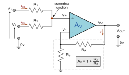
Fig 14: Non-Inverting Summing Amplifier
Applying KCL to the above circuit we have IR1+IR2 = 0
When R1 = R2 =R V+ = The voltage gain for non-inverting summing amplifier is given as AV = Vout/Vin = Vout= [1+ |
Key takeaways
- AV = Vout/Vin =
 = 1+
= 1+
- Vout= [1+
 ]
] 
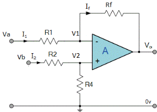
Fig 15: Difference amplifier
- Here input can be provided simultaneously at both the terminals of amplifier.
- Voltage signal Va is applied at one input terminal and another voltage signal Vb onto the other input terminal then resultant output voltage is proportional to the “Difference” between the input voltages Va and Vb.
- Vo = Vb - Va
- Now by applying superposition theorem we get,


Summing point, V1 = V2 and
V2 = Vb
If Vb = 0 then
And Va = 0 then
Vo = -V01 + V02
Vo =
If R1 = R2 and Rf = R4 then
And if R1 = R2 = Rf = R4 =R then
Vo = Vb – Va
|
Hence, is known as a Unity Gain Differential Amplifier.
Key takeaways
- The output of subtractor is

1. Ramakant. A. Gayakwad, “Op-Amps & Linear Integrated Circuits”, 3rd Edition, PHI
2. S.Salivahanan&Bhaaskaran, “Linear Integrated Circuits”, 1st Edition, Tata McGraw Hill.
3. T.R Ganesh Babu, “Linear Integrated Circuits”, 3rd Edition, SciTech Publication
4. Sergio Franco, “Design with op-amp &Analog Integrated Circuits”, 3rd Edition, Tata McGraw Hill
5. “Operational Amplifiers and Linear IC’s”, David A. Bell, 2
nd edition, PHI/Pearson, 2004
6. “Linear Integrated Circuits”, D. Roy Choudhury and Shail B. Jain, 2nd edition, Reprint 2006, New Age International
