UNIT 2
Op-Amps as AC Amplifiers
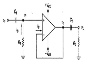
When a voltage follower is to have its input and output capacitor-coupled, the non-inverting input terminal must be grounded via a resistor. The resistor is required to pass bias current to the amplifier non-inverting input terminal. A resistor equal to R1 might be included in series with the non-inverting terminal to equalize the IBRB voltage drop and thus minimize the output offset voltage. However, in the case of a circuit with its output capacitor coupled, small dc offset voltage is unimportant because they are blocked by the capacitor.
The below shown is the figure for capacitor coupled voltage follower. In this we calculate RL, C1 and C2. To ensure minimum power dissipation largest possible values are selected.
|
Fig 1 Capacitor Coupled Voltage follower
Let Zi’ be the input impedance at non-inverting terminal of Op-amp. Then

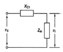
The value of resistor RL is less than R1. The capacitor value is inversely proportional to the resistance in series. At f1 lower 3db frequency the impedance of C1 has to be very less than Zin. If this condition is met there is no division of signal across XC1 and Zin as shown below. In this case, C1 will have no effect on the circuit low 3dB frequency.
|
|
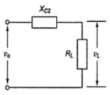
Fig 2(b) and 2(c) Signal voltage division and output voltage division
At f1 Xc1 = Thus, C1 is calculated from C1 = From fig 2(c) we can conclude that
For XC2 = RL
At 3db frequency XC2 = RL
|
As we can see that using above design method, we can use smallest possible capacitor values.
Key takeaways
- When R1 is smaller than RL, C1 would be larger capacitor than C2. To give the smallest capacitor values in this case, it is best to letC1deternine the low 3dBfrequency, by making Xc1=R1 at f1. Then Xc2 = RL/10 at f1
Example-1
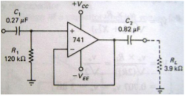
Design a capacitor-coupled voltage follower using a 741 operational amplifier. The lower cut-off frequency for the circuit is to be 50 Hz and the load resistance is RL=3.9kΩ. [Ref 4]
Sol:
= = 0.8μF |
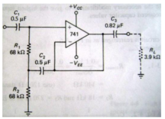
The final circuit design will be
|
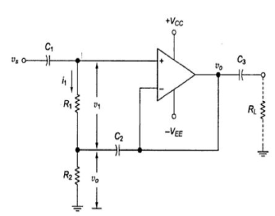
The input impedance of the capacitor-coupled voltage follower discussed previously is set by the value of the resistor R1. This gives much smaller input impedance than the direct-coupled voltage follower. Figure shows a method by which the input impedance of the capacitor-coupled voltage follower can be substantially increased. The figure below shows that the junction Resistors R1 and R2 are coupled with C2. The voltage v0 is developed across R2 because C2 acts as short circuit.
|
Fig 2 Capacitor Coupled Voltage Follower


For the circuit shown above has very high input impedance. We first calculate R1 and R2 for designing high input impedance capacitor coupled voltage follower. But the value of C2 at lower 3db frequency should be
XC2 = R2/10
The output impedance can be used to set the lower input impedance of high input impedance voltage follower.
XC3 = RL
Key takeaways
- The value of C1 should be calculated
as XC1 = Zin/10
The values of XC1 = R1/10
R1 = R2
XC1= XC2
C1= C2
Example-2
For the circuit in example-1 make the necessary changes and make it high input impedance voltage follower. Calculate input impedance of the circuit. Given A=50k Sol: R1+R2 = R1max = 140kΩ R1+R2 = 70 kΩ C3= C2 = C1= C2 = 0.5 μF Zin = (1+A) R1 = (1+50000) x 68000 = 3400MΩ |
The required circuit is
|
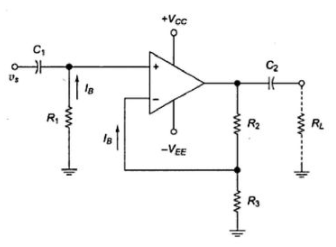
When the input of a non-inverting amplifier is to be capacitor coupled, the non-inverting input terminal must be grounded via a resistor to provide a path for the input bias current. R1 may be equal to R1||R2as in the direct-coupled case. However, as already explained, dc offset is unimportant when the output is capacitor coupled, so any reasonable value of R1 is chosen within the limit set by R1max
|
Fig 3 Capacitor Coupled Non-Inverting Amplifier
Key takeaways
1. The Zin = R1. The calculations of R2 and R3 are same as in capacitor coupled voltage amplifier.
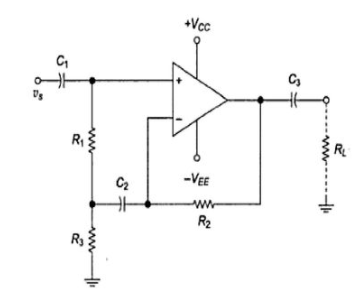
The input impedance for capacitor coupled non-inverting amplifier is very low. So, to increase the input impedance C2 is connected. The circuit is shown below.
|
Fig 4 High Input Impedance Capacitor Coupled Non-Inverting Amplifier
The voltage feedback from the output to the input is reduced in this case by
|
The capacitor values can be exactly as for the high input impedance voltage follower. An alternative to this for a circuit which might have a variable load is to use C2 to determine the low 3dB frequency for the circuit. With C2 in the circuit, the voltage gain is
Av = For XC2 = R3 Av = |
Key takeaways
1. The assumption XC2 << (R2+R3) is valid only when XC2 = R3 and R3<<R2 which is the case when circuit has substantial voltage gain.
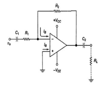
A capacitor-coupled inverting amplifier is the figure. In this case, bias current to the op-amp inverting input terminal flows via resistor R2, so coupling capacitor C1 does not interrupt the input bias current. No resistor is included in with the non-inverting input terminal, because a small dc offset is unimportant with a capacitor-coupled output. If it is desired to equalize the IBRB voltage drops, the resistance in series with the non-inverting input should equal R2 because R2 is not part of the bias current path at the inverting input terminal.
|
Fig 5 Capacitor Coupled Inverting Amplifier
XC1 = R1/10 at f1
XC2 = RL at f1
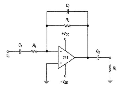
The selection of op-amp decides the highest signal frequency. When very low frequency signals are amplified and unwanted high frequency signals are to be removed then the upper cut-off frequency will be higher than the desired frequency. This can be done by connecting feedback capacitor Cf. This capacitor is connected to the inverting input and the output as shown in below figure.
|
Fig 6 Inverting Amplifier with Cf
For inverting amplifier


Key takeaways
1. It must be noted that this method of setting the circuit upper cut-off frequency is applicable only the op-amp has a much higher cut-off frequency
The values for resistors here are calculated in the same way as in direct coupled circuit and the capacitor can be calculated as
|
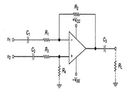
Fig 7 Capacitor Coupled Difference Amplifier
|
Key takeaways
- For the difference amplifier, capacitors should be placed across resistors R2 and R4 with each one calculated at the desired cut-off frequency as XC = (resistance in parallel).
Voltage Follower
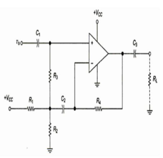
The capacitor coupled op-amp circuits can be used for single polarity supply voltage as they can block the dc bias voltages. The figure is shown below. The voltage VCC/2 is seen at the non-inverting terminal because of the potential divider circuit. The potential divider resistors are determined by choosing resistor current which is very high than the op-amp input bias current. The voltage drop across each resistor is VCC/2.
The input impedance of the circuit is
Zin = R1||R2
XC1 = (R1||R2)/10 at f1
XC2 = RL
Non-Inverting Amplifier
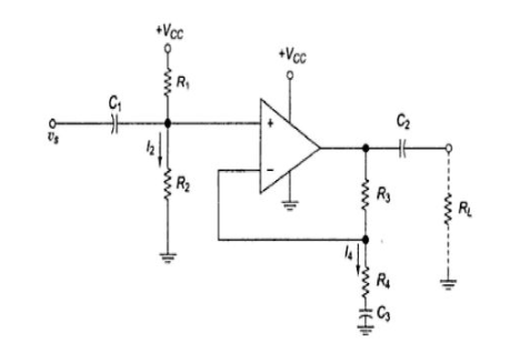
Here also due to potential divider the voltage at non-inverting input terminal is VCC/2. The capacitor C3 acts as short circuit for ac voltages. The procedure for calculating C1, C2, R1 and R2 is same as in voltage follower. The value of C3 is selected so that the value of reactance is less than R4. The circuit is shown below.
|
Fig 8 Capacitor Coupled Non-Inverting Amplifier using Single polarity supply
The Value of XC3 = R4/10. The single polarity high input impedance non-inverting amplifier is similar to high input impedance voltage follower. The circuit is shown below. The resistance R4 is connected to the non-inverting amplifier which provides the gain.
|
Fig 9 High Input Impedance Capacitor Coupled Non-Inverting Amplifier using Single polarity supply
The values of R1, R2 and capacitor values are calculated in the same manner as in non-inverting amplifiers.
Inverting Amplifier
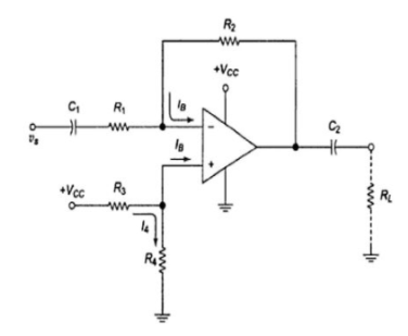
The inverting amplifier with single polarity is shown below. In this case, a potential divider (R3 and R4) is used to set the non-inverting input terminal at VCC/2. The dc voltage level of the output and the inverting input terminal will the also be VCC/2. As always, the potential divider is designed by first selecting a current (I4) which is much greater than the current flowing out of the potential divider (IB in this case).
|
Fig 10 Inverting Amplifier with Single Polarity
Then R3 = R4 = (VCC/2)/I4
The values of other parameters can be calculated in same fashion as in capacitor coupled inverting amplifier.
Key takeaways
- The capacitor coupled op-amp circuits can be used for single polarity supply voltage as they can block the dc bias voltages.
1. Ramakant. A. Gayakwad, “Op-Amps & Linear Integrated Circuits”, 3rd Edition, PHI
2. S. Salivahanan & Bhaaskaran, “Linear Integrated Circuits”, 1st Edition, Tata McGraw Hill.
3. T.R Ganesh Babu, “Linear Integrated Circuits”, 3rd Edition, SciTech Publication
4. Sergio Franco, “Design with op-amp &Analog Integrated Circuits”, 3rd Edition, Tata McGraw Hill
5. “Operational Amplifiers and Linear IC’s”, David A. Bell, 2
nd edition, PHI/Pearson, 2004
6. “Linear Integrated Circuits”, D. Roy Choudhury and Shail B. Jain, 2nd edition, Reprint 2006, New Age International
