UNIT 3
Op-Amps frequency response and compensation
The criterion for stability is used when the system is to be tested practically. In theoretically, always used to test system for stability, ex: Bode plots.
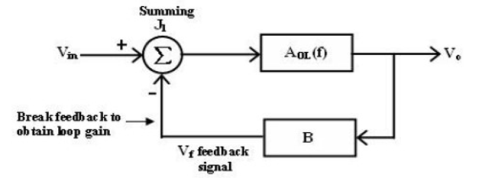
Bode plots are compared of magnitude Vs Frequency and phase angle Vs frequency. Any system whose stability is to be determined can represented by the block diagram.
|
Fig 1 Feedback loop system
The block between the output and input is referred to as forward block and the block between the output signal and f/b signal is referred to as feedback block. The content of each block is referred as transfer frequency.
From fig. we represented it by AOL (f) which is given by
AOL (f) = V0/Vin if Vf = 0 ----- (1) where AOL (f) = open loop volt gains. The closed loop gain Af is given by AF = V0/Vin = AOL / (1+(AOL) (B) ----(2) B = gain of feedback circuit. B is a constant if the feedback circuit uses only resistive components. Once the magnitude Vs frequency and phase angle Vs frequency plots are drawn, system stability may be determined as follows |
Method 1:
Determine the phase angle when the magnitude of (AOL) (B) is 0dB (or) 1.
If phase angle is >-180 , the system is stable. However, some systems the magnitude may never be 0, in that cases method 2, must be used.
Method 2:
Determine the phase angle when the magnitude of (AOL) (B) is 0dB (or) 1.
If phase angle is > - 180 , If the magnitude is –ve decibels then the system is stable. However, some systems the phase angle of a system may reach -1800, under such conditions method 1 must be used to determine the system stability.
Key takeaways
- A system is said to be unstable, if its o/p increases with time instead of achieving a fixed value.
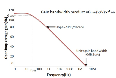
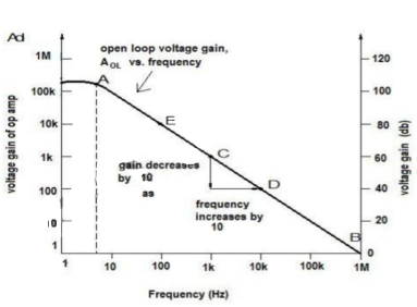
“Open Loop Gain” which is defined as the amplifiers output amplification without any external feedback signals connected to it and for a typical operational amplifier is about 100dB at DC (zero Hz). This output gain decreases linearly with frequency down to “Unity Gain” or 1, at about 1MHz and this is shown in the following open loop gain response curve.
Open-loop Frequency Response Curve
|
Fig 2 Frequency Response Curve
From this frequency response curve, we can see that the product of the gain against frequency is constant at any point along the curve. Also, that the unity gains (0dB) frequency also determines the gain of the amplifier at any point along the curve. This constant is generally known as the Gain Bandwidth Product or GBP. Therefore:
GBP = Gain x Bandwidth = A x BW For example, from the graph above the gain of the amplifier at 100kHz is given as 20dB or 10, then the gain bandwidth product is calculated as: GBP = A x BW = 10 x 100,000Hz = 1,000,000. Similarly, the operational amplifiers gain at 1kHz = 60dB or 1000, therefore the GBP is given as: GBP = A x BW = 1,000 x 1,000Hz = 1,000,000. The Voltage Gain (AV) of the operational amplifier can be found using the following formula: Av = Vout/ Vin and in Decibels or (dB) is given as: 20 log (A) or 20 log (Vout/ Vin ) in dB |
An Op- Amp Bandwidth
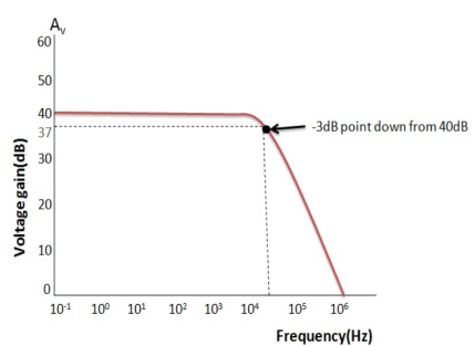
The operational amplifiers bandwidth is the frequency range over which the voltage gain of the amplifier is above 70.7% or -3dB (where 0dB is the maximum) of its maximum output value.
|
Fig 3 Frequency Response
Example-1
Using the formula 20 log (A), we can calculate the bandwidth of the amplifier as: 37 = 20 log (A) therefore, A = anti-log (37 /20) = 70.8 GBP/ A = Bandwidth, therefore, 1,000,000 / 70.8 = 14,124Hz, or 14kHz Then the bandwidth of the amplifier at a gain of 40dB is given as 14kHz as previously predicted from the graph. |
Closed loop frequency response
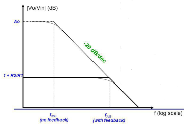
An op-amp is operated in closed loop configuration. In open loop frequency response, we know that the bandwidth is till the first break frequency. Which is the maximum useful frequency of open loop system. Due to this bandwidth is small but practically we require infinite bandwidth. The increase in bandwidth provides same gain at all frequencies. This is the reason negative feedbacks are used so that the bandwidth of op-amp can be increased.
|
Fig 4 Frequency Response of Op-Amp
The bandwidth of the operational amplifier is defined as the frequency range over which the voltage gain of the amplifier is above -3dB (maximum is 0dB) of its maximum output value. From above curve we see that the product of gain and frequency is constant at any point along the curve. This constant is known as the Gain-Bandwidth product (GB). Also, the gain of the amplifier at any point along the curve is determined by unity-gain (0 dB) frequency.
Most of the general-purpose op-amps are internally compensated by using a capacitor of the order of 30pF.The internal compensation helps in preventing the op-amp oscillating at higher frequencies. Otherwise at some higher frequencies if bark-Haussean criteria is satisfied, the op-amp may go to oscillating state. Thus op-amp is prevented from going in to oscillating state. The typical frequency response of an internally compensated would be as shown above. Since the reactance of the capacitor=1/(2πfc), as the frequency increases by 10, the capacitor reactance decreases by 10.A change in frequency of 10 is called decade.
|
Fig 5 Frequency Response of Internally Compensated Op-Amp
In the above plot, a represents the break frequency at which the gain of the op-amp is 0.707 times the gain at the lower frequencies. Points C and D shows how gain decreases by 10 as the frequency increases by 10. Thus, to express the slope of the response usually we use the term per decade. The right-hand vertical axis in the plot shows the value of the gain in db. The voltage gains decrease by 20 dB for every 1 decade increases in frequency, thus we say that the response is rolling off at 20dB/decade.
Key takeaways
- “Open Loop Gain” which is defined as the amplifiers output amplification without any external feedback signals connected to it and for a typical operational amplifier is about 100dB at DC (zero Hz).
Lead Compensation
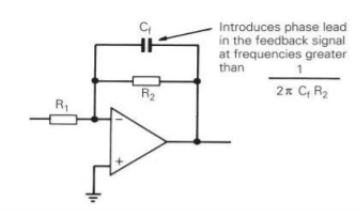
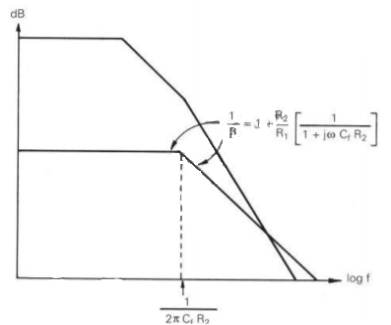
Lead frequency compensation is a technique used to increase the phase margin. A capacitor is included in a feedback loop to introduce a phase lead, compensating for the op-amp phase lag which would otherwise result in insufficient phase margin. A simple way of achieving this is to connect a capacitor Cf in parallel with the feedback resistance. A circuit using this method of lead compensation is shown, together with its associated Bode plots, in Figure
|
|
Fig 6 Compensation using capacitor and Bode Plot.
At frequencies greater than 1/2 CfR2 the capacitor introduces a phase lead in the feedback fraction, which approaches 90S. If Cf is chosen so that the frequency 1/2
 CfR2 is a decade below the frequency at which open-loop response plots intersect, a phase margin of approximately 90S is obtained. Use of a lead capacitor in parallel with a feedback resistor is a convenient way of getting extra phase margin. It is also a technique that can be used to overcome the effect of stray capacitance between the op-amp’s inverting input and earth.
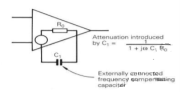
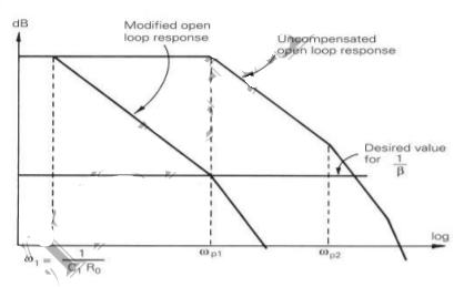
Shunting a signal point with a capacitor resistor combination (a lag network) is an alternative technique that allows wider closed-loop bandwidths. At frequencies above 1/2 C1R1 (the break-back frequency) a network of this kind produces an attenuation R1/(R1||Ro) but the phase shift returns to zero.
|
|
Fig 7 Simple lag compensation with single capacitor
Previous sections have been concerned with factors influencing the small signal frequency response characteristics of op-amp feedback circuits. Attention is now directed to the factors influencing their behaviour in time, namely their transient behaviour in response to large and small input step or square-wave signals. Students may gain a greater understanding of op-amp transient behaviour, and the terminology used to describe it, by performing transient tests. Frequency compensating component magnitude, load capacitance, input capacitance and any stray feedback capacitance all influence closed-loop transient behaviour.
Key takeaways
- Lead frequency compensation is a technique used to increase the phase margin. A capacitor is included in a feedback loop to introduce a phase lead.
An op-amp is operated in closed loop configuration. In open loop frequency response, we know that the bandwidth is till the first break frequency. Which is the maximum useful frequency of open loop system. Due to this bandwidth is small but practically we require infinite bandwidth. The increase in bandwidth provides same gain at all frequencies. This is the reason negative feedbacks are used so that the bandwidth of op-amp can be increased.
The bandwidth of the operational amplifier is defined as the frequency range over which the voltage gain of the amplifier is above -3dB (maximum is 0dB) of its maximum output value. From above curve we see that the product of gain and frequency is constant at any point along the curve. This constant is known as the Gain-Bandwidth product (GB). Also, the gain of the amplifier at any point along the curve is determined by unity-gain (0 dB) frequency.
The slew rate is a parameter that describes the operating speed of an op-amp. It represents the rate that can change per unit time stipulated by the output voltage.
For example, 1V/us indicates that the voltage can change by 1V in 1μs. Ideal op-amps make it possible to faithfully output an output signal for any input signal. However, in reality slew rate limits do exist.
When supplying a rectangular pulse at the input with a steep rise and fall, this indicates the possible degree of change in the output voltage per unit time.
|
Fig 8 Slew Rate calculation
The rise and fall slew rates are calculated by the following equations:
SRr = ∆ V / ∆ Tr
SRf = ∆ V / ∆ Tf
|
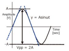
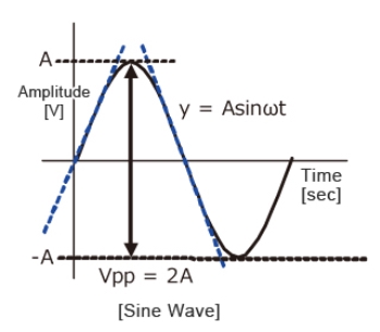
Fig 9 Sinusoidal waveform
Calculate the slew rate
The output is given by
y=Asinωt
The slew rate is the slope of the tangent of the sine wave, differentiating the above equation.
dy | / = Aω cosωt |
| ωt=0 |
Dt |
The slew rate is
SR=Aω ω=2πf
|
Fig 10 Sinusoidal Waveform
Since the amplitude of the sine wave becomes Vpp=2A (peak-to-peak), the equation can be modified as follows.
|
|
|
|
|
|
|
|
|
This frequency(f) is referred to as the full power bandwidth. These are conditions where the amplification factor in the op-amp has not been set, in other words the relationship of the frequency and amplitude (within the output voltage range) that can be output by the op-amp in a voltage follower circuit.
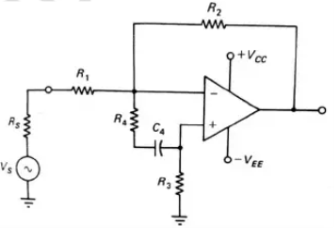
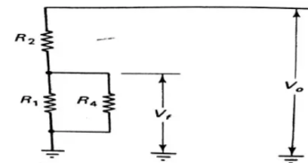
Zin Mod compensation
very less than the resistance R4 at the frequency at which M =1. The feedback network changed by Zin Mod is shown below.
|
Fig 11 Zin Mod Compensation
|
Fig 12 Network neglecting Rs and R3
Now, the feedback factor without R4 and C4 will become
When R4 is considered the feedback factor in the circuit becomes
The gain of op-amp is
The voltage gains for inverting amplifier is
Without R4 and C4 the gain of amplifier is Av = 1/
|
Circuit Stability Precautions
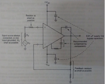
The instability in the op-amp is due to the feedback along the supply line. This can be reduced by connecting 0.01μF high frequency supply decoupling capacitors from each supply terminal to ground.
|
Fig 13 Circuit Stability Circuit
The basic precautions required are listed below.
- For low frequency operations we should use internally compensated op-amp like 741.
- The leads should be kept small for all the components used.
- The op-amp input terminal should have the body of the resistor placed close to the input terminal.
- The 0.01μF high frequency supply decoupling capacitors from each supply terminal to ground should be used.
- There should not be any instruments connected to both the terminals of op-amp.
- Always have a single source connected to a circuit to be tested.
- If the circuit bandwidth is not large with the recommended compensation technique, we may use Zin Mod.
Key takeaways
- Slew rate is the maximum rate of output voltage change per unit time. It is denoted by S. For getting undistorted output voltage we must have very high slew rate. It is measured in V/sec.
1. Ramakant. A. Gayakwad, “Op-Amps & Linear Integrated Circuits”, 3rd Edition, PHI
2. S.Salivahanan & Bhaaskaran, “Linear Integrated Circuits”, 1st Edition, Tata McGraw Hill.
3. T.R Ganesh Babu, “Linear Integrated Circuits”, 3rd Edition, SciTech Publication
4. Sergio Franco, “Design with op-amp &Analog Integrated Circuits”, 3rd Edition, Tata McGraw Hill
5. “Operational Amplifiers and Linear IC’s”, David A. Bell, 2
nd edition, PHI/Pearson, 2004
6. “Linear Integrated Circuits”, D. Roy Choudhury and Shail B. Jain, 2nd edition, Reprint 2006, New Age International
