UNIT 4
OP-AMP Applications
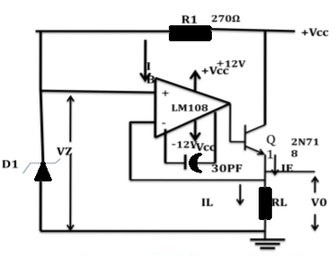
Low Resistance Voltage Source
Because the maximum output current that can be supplied by most operational amplifiers is approximately 25 mA, the transistor is necessary for higher load current levels.
The maximum load current is maximum emitter current for the transistor, and the op-amp has only to supply the much smaller transistor base current.
In fig instead of using a potential divider to provide the desired reference voltage, a Zener diode can be employed.
Zener diode is largely independent of any variations in supply voltage.
|
Fig 1 Voltage Derived from Zener Diode
Precision Voltage Source
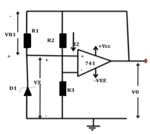
The circuit shown in figure below uses the output voltage to maintain a constant current through the diode, thus providing a precise unchanging voltage, and consequently, a precise output level.
In figure both the Zener diode circuit (D1 and R1) and the potential divider (R2 and R3) are supplied from the op-amp output terminal. Suppose the z\Zener diode voltage is 4.5V and the voltage drop across R1 is 4.5V.
The total voltage drops across D1 and R1 is 9V. This is also the output voltage V0
|
Fig 2 Precision Voltage Source
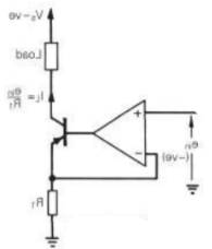
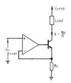
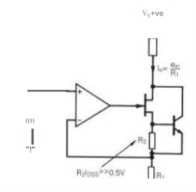
The voltage-to-current sources considered so far have provided a bi-directional output current. Unidirectional current sources can be formed using a simple circuit comprising a transistor, a resistor and an op-amp, as shown in Figure. Resistor R1 is a current sensing resistor. Feedback around the op-amp forces the current through resistor R1 to take on a value such that I1=ein/ R1. The current I1 is the emitter current of the transistor, less the very small bias current of the op-amp. The collector current of the transistor, which is almost equal to its emitter current, forms the stable output current to the load. Output currents greater than the capability of the op-amp are possible, since the op-amp need only supply the output transistor’s base current. A current limit is set by transistor saturation caused by the voltage that appears across the load. Departure from linearity in voltage-to-current conversion is likely at low current levels. This is because the gain of a bipolar transistor falls at low values of collector current.
|
Fig 3 Current Source
|
Fig 4 Current Sink
|
Fig 5 Precise current sink
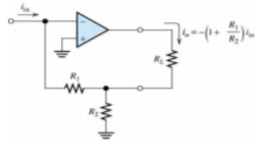
The linearity dependence on transistor current gain, exhibited by the current sources of Figure, can be overcome by using a FET in place of the bipolar transistor. However, output current is then limited to the Idss of the FET. The output current limit can be overcome by combining an n-channel FET and a bipolar npn transistor as shown in Figure. In the circuit given in Figure, virtually all the current through the sensing resistor R1 flows as output current. The only error contributions being the very small gate leakage current and the op-amp bias current.
|
Fig 6 Current Amplifier
Avi = -(1+R2/R1)
Zin =0
Zout = ∞
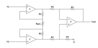
This instrumentation amplifier provides high input impedance for exact measurement of input data from transducers. The circuit diagram of an instrumentation amplifier is as shown in the figure below.
|
Fig 7 Instrumentation Amplifier
The op-amps 1 & 2 are non-inverting amplifiers and together form an input stage of the instrumentation amplifier. The op-amp 3 is a difference amplifier that forms the output stage of the instrumentation amplifier.
Working
The output stage of the instrumentation amplifier is a difference amplifier, whose output Vout is the amplified difference of the input signals applied to its input terminals.
If the outputs of op-amp 1 and op-amp 2 are Vo1 and Vo2 respectively, then the output of the difference amplifier is given by,
Vout = (R3/R2) (Vo1-Vo2)
The expressions for Vo1 and Vo2 can be found in terms of the input voltages and resistances.
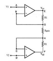
Consider the input stage of the instrumentation amplifier as shown in the figure below.
|
Fig 8 Input Stage of Instrumentation Amplifier
The potential at node A is the input voltage V1. Hence the potential at node B is also V1, from the virtual short concept. Thus, the potential at node G is also V1.
The potential at node D is the input voltage V2. Hence the potential at node C is also V2, from the virtual short. Thus, the potential at node H is also V2.
Ideally the current to the input stage op-amps is zero. Therefore, the current I through the resistors R1, Rgain and R1 remains the same.
Applying Ohm’s law between the nodes E and F, I = (Vo1-Vo2)/(R1+Rgain+R1) ——————— 1 I = (Vo1-Vo2)/(2R1+Rgain) Since no current is flowing to the input of the op-amps 1 & 2, the current I between the nodes G and H can be given as, I = (VG-VH)/Rgain = (V1-V2)/Rgain ————————- 2 Equating equations 1 and 2, (Vo1-Vo2)/(2R1+Rgain) = (V1-V2)/Rgain (Vo1-Vo2) = (2R1+Rgain) (V1-V2)/Rgain —————— 3 The output of the difference amplifier is given as, Vout = (R3/R2) (Vo1-Vo2) Therefore, (Vo1 – Vo2) = (R2/R3) Vout Substituting (Vo1 – Vo2) value in the equation 3, we get (R2/R3) Vout = (2R1+Rgain) (V1-V2)/Rgain i.e. Vout = (R3/R2) {(2R1+Rgain)/Rgain} (V1-V2) |
The above equation gives the output voltage of an instrumentation amplifier. The overall gain of the amplifier is given by the term (R3/R2) {(2R1+Rgain)/Rgain}.
- The gain of a three op-amp instrumentation amplifier circuit can be easily varied and controlled by adjusting the value of Rgain without changing the circuit structure.
- The gain of the amplifier depends only on the external resistors used. Hence, it is easy to set the gain accurately by choosing the resistor values carefully.
- The input impedance of the instrumentation amplifier is dependent on the non-inverting amplifier circuits in the input stage. The input impedance of a non-inverting amplifier is very high.
- The output impedance of the instrumentation amplifier is the output impedance of the difference amplifier, which is very low.
- The CMRR of the op-amp 3 is very high and almost all of the common mode signal will be rejected.
Key takeaways
- This instrumentation amplifier provides high input impedance for exact measurement of input data from transducers. The output impedance of the instrumentation amplifier is the output impedance of the difference amplifier, which is very low.
|
Fig 9 Precision Rectifier
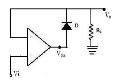
The below figure shows a non-inverting precision rectifier. The diode used is called as precision diode. When the voltage VI is positive the voltage VOA is also positive. When Vi<0the voltage VOA becomes negative and hence reverse biasing the diode and making Vo =0.
When the value of input voltage Vi< (cut-in voltage). The diode again becomes reverse biased as VOA becomes negative. The op-amp then comes to negative saturation. There is no current through RL and V0= 0.
When the value of input voltage Vi> (cut-in voltage) the circuit acts as voltage follower and the output voltage follows the input voltage during this positive half cycle of input.
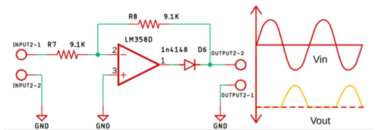
|
Fig 10 Input and Output of Precision Rectifier
|
Fig 11 Half wave precision rectifier circuit.
|
Fig 12 When positive and negative half cycle of input signal is applied to Op-amp
Full wave precision rectifier circuit
Fig 13 Precision Full Wave Rectifier
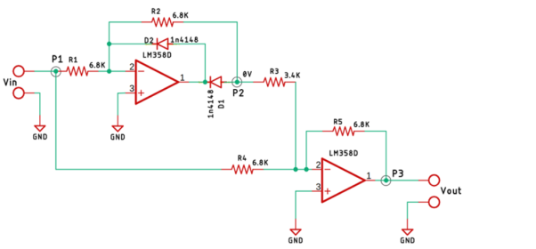
In full wave summing amplifier is added at the output. From the point, P1 to point P2 is the basic precision rectifier circuit and the diode is so configured that we get a negative voltage at the output.
From the point, P2 to point P3 is the summing amplifier, the output from the precision rectifier is fed to the summing amplifier through the resistor R3.
The input from the point P1 is also fed to the summing amplifier with the help of the resistor R4, the resistors R4 and R5 are responsible for setting the gain of the op-amp to 1X.
Since the output from the Point P2 is fed directly to the summing amplifier with the gain of 2X, that means the output voltage will be 2-times the input voltage. The output is obtained at P3.
Key takeaways
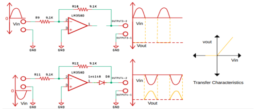
- The precision diode operates in first quadrant when Vi>0 and V0>0. The precision diode operates in third quadrant when diode is connected in reverse bias.
|
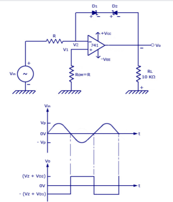
Fig 14 Voltage limiter
In the figure shown above, there are two Zener diodes that are connected in the feedback path of the op-amp circuit. This design helps in keeping the voltage limit between the positive and negative values of the output voltage, V0. As shown in the waveform, as the voltage Vin increases from 0 to positive voltage, the value of V0 increases in the opposite direction (negative). This goes on until the diode D1 becomes forward biased and D2 goes into avalanche breakdown.
V0 = VZ + VD1 VZ – Zener Voltage VD1 – Voltage drop across D1 = 0.7V |
If Vo increases from 0 to negative voltage, Vo increases positively until diode D2 is forward biased and D1 goes into avalanche condition.
|
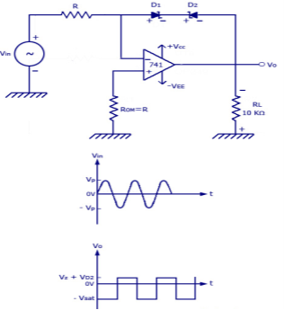
Fig 15 Positive output voltage limiting
V0 = VZ + VD2 VZ – Zener Voltage VD1 – Voltage drop across D2 = 0.7V Thus the limit of output voltage swing is between +(VZ + 0.7) and – (VZ + 0.7).
since the v1=v2=0V (virtual ground). The figure above shows a combination of zener diode and rectifier diodes. This circuit is used to bring the level of swing of V0 to a positive direction. When Vin ranges from 0 to positive voltage, D2 is reverse biased and thus V0 = -Vsat. When Vin ranges from 0 to negative voltage, D2 is forward biased and D1 goes into avalanche condition. Thus V0 = VZ + VD2.
|
References:
1. Ramakant. A. Gayakwad, “Op-Amps & Linear Integrated Circuits”, 3rd Edition, PHI
2. S. Salivahanan & Bhaaskaran, “Linear Integrated Circuits”, 1st Edition, Tata McGraw Hill.
3. T.R Ganesh Babu, “Linear Integrated Circuits”, 3rd Edition, SciTech Publication
4. Sergio Franco, “Design with op-amp &Analog Integrated Circuits”, 3rd Edition, Tata McGraw Hill
5. “Operational Amplifiers and Linear IC’s”, David A. Bell, 2
nd edition, PHI/Pearson, 2004
6. “Linear Integrated Circuits”, D. Roy Choudhury and Shail B. Jain, 2nd edition, Reprint 2006, New Age International
