UNIT 5
More applications
A clamper is an electronic circuit that produces an output, which is similar to the input but with a shift in the DC level. In other words, the output of a clamper is an exact replica of the input. Hence, the peak to peak amplitude of the output of a clamper will be always equal to that of the input.
Positive Clamper
A positive clamper is a clamper circuit that produces an output in such a way that the input signal gets shifted vertically by a positive DC value.
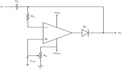
The circuit diagram of a positive clamper is shown in the following figure
|
Fig 1 Positive Clamper Circuit
In the above circuit, a sinusoidal voltage signal, Vi is applied to the inverting terminal of op-amp through a network that consists of a capacitor C1 and a resistor R1. That means, AC voltage signal is applied to the inverting terminal of the op-amp.
The DC reference voltage Vref is applied to the non-inverting terminal of the op-amp. The value of reference voltage Vref can be chosen by varying the resistor R2. In this case, we will get a reference voltage Vref of a positive value.
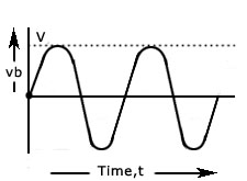
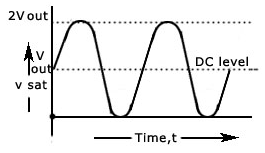
The above circuit produces an output, which is the combination of the sinusoidal voltage signal Vi and the reference voltage Vref. That means, the clamper circuit produces an output in such a way that the sinusoidal voltage signal Vi gets shifted vertically upwards by the value of reference voltage Vref.
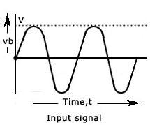
The input wave form and the corresponding output wave form of positive clamper are shown in above figure
|
|
Fig 2 Input and Output waveform of positive clamper
Negative Clamper
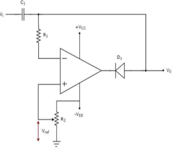
A negative clamper is a clamper circuit that produces an output in such a way that the input signal gets shifted vertically by a negative DC value.
|
Fig 3 Negative Clamper
In the above circuit, a sinusoidal voltage signal Vi is applied to the inverting terminal of the op-amp through a network that consists of a capacitor C1 and resistor R1. That means, AC voltage signal is applied to the inverting terminal of the op-amp.
The DC reference voltage Vref is applied to the non-inverting terminal of the op-amp. The value of reference voltage Vref can be chosen by varying the resistor R2. In this case, we will get reference voltage Vref of a negative value.
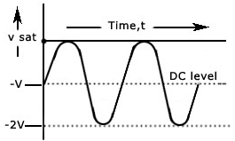
The above circuit produces an output, which is the combination of sinusoidal voltage signal Vi and reference voltage Vref. That means, the clamper circuit produces an output in such a way that the sinusoidal voltage signal Vi gets shifted vertically downwards by the value of reference voltage Vref.
|
|
Fig 4 Input and Output waveform of Negative Clamper
Key takeaways
- A positive clamper produces an output in such a way that the sinusoidal voltage signal Vi gets shifted vertically upwards by the value of reference voltage Vref.
- A negative clamper produces an output in such a way that the sinusoidal voltage signal Vi gets shifted vertically downwards by the value of reference voltage Vref.
|
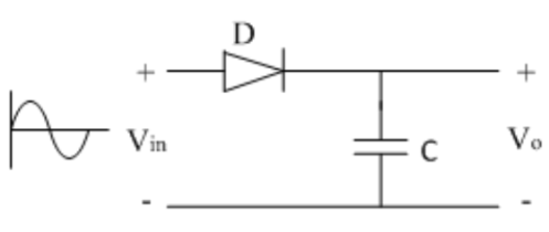
Fig 5 Peak detector
In the positive half cycle, diode D is forward biased and capacitor C starts charging. When input reaches its peak value, capacitor gets charged to positive peak value.
In negative half cycle, as input decreases, diode D is reversed biased and capacitor is isolated and holds the peak value of previous cycle. Hence called as peak detector.
But in practice, output is taken across some load RL, so when input voltage decreases capacitor discharges through load RL. To avoid this, select RL of very large value so that capacitor discharges very slowly hence almost hold the charge. Whatever charge it lost through RL is gets back in next half cycle.
Key takeaways
- The diode D is acting as an instant switch, so supply gets loaded. To avoid the loading while charging capacitor, we use op-amp.
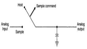
- The Sample and Hold circuit is an electronic circuit which creates the samples of voltage given to it as input, and after that, it holds these samples for the definite time. The time during which sample and hold circuit generates the sample of the input signal is called sampling time.
- Similarly, the time duration of the circuit during which it holds the sampled value is called holding time.
- Sampling time is generally between 1µs to 14 µs while the holding time can assume any value as required in the application.
- It will not be wrong to say that capacitor is the heart of sample and hold circuit.
- This is because the capacitor present in it charges to its peak value when the switch is opened, i.e during sampling and holds the sampled voltage when the switch is closed.
Need for Sample and Hold Circuits
If the input analog voltage of an ADC changes more than ±1/2 LSB, then there is a severe chance that the output digital value is an error. For the ADC to produce accurate results, the input analog voltage should be held constant for the duration of the conversion.
It is based on a sampling command and holds the output value at its output until the next sampling command is arrived.
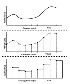
The following image shows the input and output of a typical Sample and Hold Circuit.
|
Fig 6 Input and output of S/H circuit
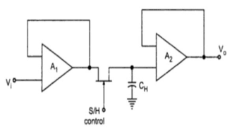
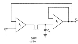
This sample and hold circuit consist of two basic components:
- Analog Switch
- Holding Capacitor
|
|
Fig 7 Open loop s/h circuit
|
Fig 8 Closed loop s/h circuit
|
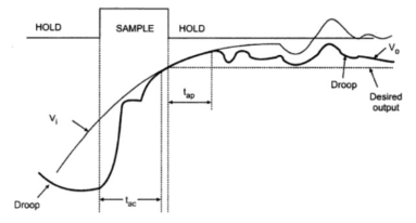
Fig 9 S/H characteristics
Acquisition Time (tac)
The time required for the charge in the holding capacitor to rise up to a level that is close to the input voltage during the sampling is called acquisition time. It is affected by three factors:
- The RC Time Constant
- The Slew-Rate of the Op-Amp
- The maximum output current of the Op-Amp
Aperture Time (tap)
The time delay between the initiation of VO tracking the Vi and the initiation of the hold command is called the Aperture Time. This delay is usually due to the propagation delays through the driver and the switch circuits.
For a precise timing operation, the hold command must be initiated in advance by an amount of aperture time.
Aperture Uncertainty (∆ tap)
The Aperture time will not be the same for all the sample and will vary from sample to sample. This uncertainty is called Aperture Uncertainty. This will severely affect the advancing of the hold command.
Hold Mode Settling Time (ts)
The hold mode settling time is the time taken by the output VO to settle within the specified error band (usually 1%, 0.1% or 0.01%) after the application of hold command.
Hold Step
During the switching from sample mode to hold mode, there might an unwanted transfer of charge between the switch and the holding capacitor (mainly due to the parasitic capacitances). This will affect the capacitor voltage as well as the output voltage. This change in the output voltage from the desired voltage is called Hold Step.
Feedthrough
Again, the parasitic capacitances in the switch may cause AC coupling between VO and Vi in hold mode. As a result, the output voltage may vary with changes in the input voltage and this is referred to as feedthrough.
Droop
Voltage Droop is a phenomenon where the voltage across the holding capacitor drops down due to leakage currents.
Advantages
- The main and important advantage of a typical SH Circuit is to aid an Analog to Digital Conversion process by holding the sampled analog input voltage.
- In multichannel ADCs, where synchronization between different channels is important, an SH circuit can help by sampling analog signals from all the channels at the same time.
- In multiplexed circuits, the crosstalk can be reduced with an SH circuit.
Key takeaways
- They are used in
- Analog to Digital Converter Circuits (ADC)
- Digital Interface Circuits
- Operational Amplifiers
- Analog De-multiplexers
- Data distribution systems
- Storage of outputs of multiplexers
- Pulse Modulation Systems
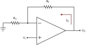
A voltage to current converter or V to I converter, is an electronic circuit that takes current as the input and produces voltage as the output.
An op-amp based voltage to current converter produces an output current when a voltage is applied to its non-inverting terminal. The circuit diagram of an op-amp based voltage to current converter is shown in the following figure.
|
Fig 10 V-I Converter
In the circuit shown above, an input voltage Vi is applied at the non-inverting input terminal of the op-amp.
According to the virtual short concept, the voltage at the inverting input terminal of an op-amp will be equal to the voltage at its non-inverting input terminal.
So, the voltage at the inverting input terminal of the op-amp will be Vi.
The nodal equation at the inverting input terminal's node is −
ViR1−I0=0 =>I0=VtR1 Thus, the output current I0 of a voltage to current converter is the ratio of its input voltage Vi and resistance R1. We can re-write the above equation as − I0/Vi=1/R1 |
The above equation represents the ratio of the output current I0 and the input voltage Vi & it is equal to the reciprocal of resistance R1. The ratio of the output current I0 and the input voltage Vi is called as Transconductance.
Current to voltage converter
A current to voltage converter or I to V converter is an electronic circuit that takes current as the input and produces voltage as the output.
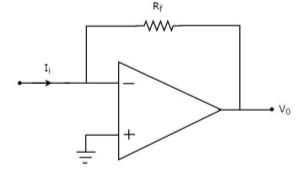
An op-amp based current to voltage converter produces an output voltage when current is applied to its inverting terminal. The circuit diagram of an op-amp based current to voltage converter is shown in the following figure.
|
Fig 11 I-V Converter
In the circuit shown above, the non-inverting input terminal of the op-amp is connected to ground. That means zero volts is applied at its non-inverting input terminal.
According to the virtual short concept, the voltage at the inverting input terminal of an op-amp will be equal to the voltage at its non-inverting input terminal. So, the voltage at the inverting input terminal of the op-amp will be zero volts.
The nodal equation at the inverting terminal's node is −
−Ii+0−V0/Rf=0
−Ii=V0/Rf
V0=−Rf.Ii
Thus, the output voltage, V0 of current to voltage converter is the (negative) product of the feedback resistance, Rf and the input current, It. Observe that the output voltage, V0 is having a negative sign, which indicates that there exists an 1800 phase difference between the input current and output voltage.
We can re-write the above equation as −
V0/Ii=−Rf
The above equation represents the ratio of the output voltage V0 and the input current Ii, and it is equal to the negative of feedback resistance, Rf. The ratio of output voltage V0 and input current Ii is called as Trans-resistance.
Key takeaways
A voltage to current converter or V to I converter, is an electronic circuit that takes current as the input and produces voltage as the output.
An op-amp based voltage to current converter produces an output current when a voltage is applied to its non-inverting terminal.
A current to voltage converter or I to V converter is an electronic circuit that takes current as the input and produces voltage as the output.
An op-amp based current to voltage converter produces an output voltage when current is applied to its inverting terminal.
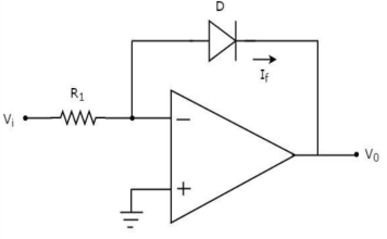
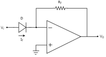
Log Amplifier
|
Fig 12 Log Amplifier
The equation for input voltage will be
If = The current flowing through diode is given as
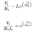
Where: Is = Saturation Current Vf = Voltage drop across diode in forward bias VT = Thermal equivalent voltage For feedback loop the KVL equation will be 0-Vf -V0 = 0 Vf = -V0 Substituting Vf in above equation of If
Equating both equations of If
Taking natural log of both sides we get
The above equations show that the output is natural log of the applied input. |
Antilog Amplifier
|
Fig 13 Antilog Amplifier
Applying KCL at input terminal we get
The current flowing through diode is given as
Substituting If in above voltage equation we get
At inverting terminal applying KVL we get
Substituting Vf in equation of V0 we get
The above equations show that the output is natural antilog of the applied input. |
Key takeaways
- For Log Amplifier

2. For Antilog Amplifier

|
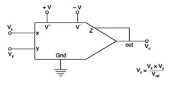
Fig 14 Multiplier
The output voltage is written as
V0 = (Vx x Vy)/Vref
If both the inputs are positive the multiplier is called one-quadrant multiplier. If one input is kept at a positive value and other at any one may be positive or negative, then it is called as two-quadrant multiplier. If both inputs are allowed to be either positive or negative, then it is called as four-quadrant multiplier.
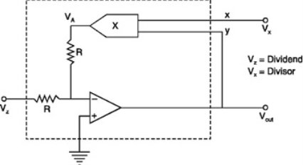
Divider
The output is given as
Vout = -Vref (Vz/Vx)
|
Fig 15 Divider
The application of divider includes square root and dividing one number by another.
Key takeaways
- The multipliers are used for frequency doubling, frequency shifting, phase angle detection and real power computation
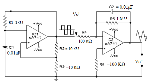
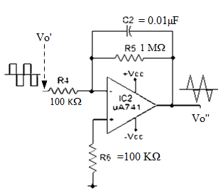
The op-amp IC used in this stage is also uA741 (IC2). Resistor R5 in conjunction with R4 sets the gain of the integrator and resistor R5 in conjunction with C2 sets the bandwidth. The square wave signal is applied to the inverting input of the op-amp through the input resistor R4. The op-amp integrator part of the circuit is shown in the figure below.
|
Fig 16 Triangular waveform generator
After this initial “kick” the capacitor starts charging and it creates an opposition to the input current flowing through the input resistor R4. The negative feedback compels the op-amp to produce a voltage at its out so that it maintains the virtual ground at the inverting input.
Since the capacitor is charging its impedance Xc keeps increasing and the gain Xc2/R4 also keeps increasing. This results in a ramp at the output of the op-amp that increases in a rate proportional to the RC time constant (T=R4C2) and this ramp increases in amplitude until the capacitor is fully charged.
When the input to the integrator (square wave) falls to the negative peak the capacitor quickly discharges through the input resistor R4 and starts charging in the opposite polarity.
Now the conditions are reversed, and the output of the op-amp will be a ramp that is going to the negative side at a rate proportional to the R4R2 time constant. This cycle is repeated, and the result will be a triangular waveform at the output of the op-amp integrator.
Key takeaways
- Since the capacitor is charging its impedance Xc keeps increasing and the gain Xc2/R4 also keeps increasing. This results in a ramp at the output of the op-amp that increases in a rate proportional to the RC time constant (T=R4C2) and this ramp increases in amplitude until the capacitor is fully charged.
|
Fig 17 Square waveform generator
Square wave generator
The square wave generator is based on a uA741 opamp (IC1). Resistor R1 and capacitor C1 determines the frequency of the square wave. Resistor R2 and R3 forms a voltage divider setup which feedbacks a fixed fraction of the output to the non-inverting input of the IC.
- Initially, when power is not applied the voltage across the capacitor C1 is 0. When the power supply is switched ON, the C1 starts charging through the resistor R1 and the output of the op-amp will be high.
- A fraction of this high voltage is fed back to the non- inverting pin by the resistor network R2, R3. When the voltage across the charging capacitor is increased to a point the voltage at the inverting pin is higher than the non-inverting pin, the output of the op-amp swings to negative saturation (-Vcc).
- The capacitor quickly discharges through R1 and starts charging in the negative direction again through R1.
- Fraction of the negative high output (-Vcc) is fed back to the non-inverting pin by the feedback network R2, R3. When the voltage across the capacitor has become so negative that the voltage at the inverting pin is less than the voltage at the non-inverting pin, the output of the op-amp swings back to the positive saturation.
- Now the capacitor discharges trough R1 and starts charging in positive direction. This cycle is repeated over time and the result is a square wave swinging between +Vcc and -Vcc at the output of the op-amp.
If the values of R2 and R3 are made equal, then the frequency of the square wave can be expressed using the following equation
F = 1/ (2.1976 R1C1)
Triangular wave generator
The op-amp IC used in this stage is also uA741 (IC2). Resistor R5 in conjunction with R4 sets the gain of the integrator and resistor R5 in conjunction with C2 sets the bandwidth. The square wave signal is applied to the inverting input of the op-amp through the input resistor R4. The op-amp integrator part of the circuit is shown in the figure below.
|
Fig 18 Triangular waveform generator
After this initial “kick” the capacitor starts charging and it creates an opposition to the input current flowing through the input resistor R4. The negative feedback compels the op-amp to produce a voltage at its out so that it maintains the virtual ground at the inverting input.
Since the capacitor is charging its impedance Xc keeps increasing and the gain Xc2/R4 also keeps increasing. This results in a ramp at the output of the op-amp that increases in a rate proportional to the RC time constant (T=R4C2) and this ramp increases in amplitude until the capacitor is fully charged.
When the input to the integrator (square wave) falls to the negative peak the capacitor quickly discharges through the input resistor R4 and starts charging in the opposite polarity.
Now the conditions are reversed, and the output of the op-amp will be a ramp that is going to the negative side at a rate proportional to the R4R2 time constant. This cycle is repeated, and the result will be a triangular waveform at the output of the op-amp integrator.
|
Fig 19 Phase Shift Oscillator
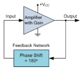
In an RC Oscillator circuit, the input is shifted 180o through the feedback circuit returning the signal out-of-phase and 180o again through an inverting amplifier stage to produces the required positive feedback.
This then gives us “180o + 180o = 360o” of phase shift which is effectively the same as 0o, thereby giving us the required positive feedback.
In other words, the total phase shift of the feedback loop should be “0” or any multiple of 360o to obtain the same effect.
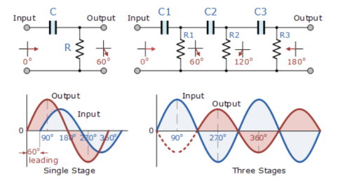
|
Fig 20 Circuit Diagram and Output waveform for single and three stage circuit
The circuit on the left shows a single resistor-capacitor network whose output voltage “leads” the input voltage by some angle less than 90o.
In a pure or ideal single-pole RC network. it would produce a maximum phase shift of exactly 90o, and because 180o of phase shift is required for oscillation, at least two single-poles networks must be used within an RC oscillator design.
However, in reality it is difficult to obtain exactly 90o of phase shift for each RC stage so we must therefore use more RC stages cascaded together to obtain the required value at the oscillation frequency.
The amount of actual phase shift in the circuit depends upon the values of the resistor (R) and the capacitor (C), at the chosen frequency of oscillations with the phase angle (φ) being given as:
Xc = 1/2π fc R=R
Z = [ R 2 + Xc 2] ½
Ø = tan -1 Xc /R
Key takeaways
- In an RC Oscillator circuit, the input is shifted 180o through the feedback circuit returning the signal out-of-phase and 180o again through an inverting amplifier stage to produces the required positive feedback.
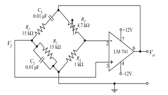
Wien bridge oscillator is an audio frequency sine wave oscillator of high stability and simplicity. The feedback signal in this circuit is connected to the non-inverting input terminal so that the op-amp is working as a non-inverting amplifier.
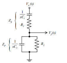
The feedback network does not provide any phase shift. The circuit can be viewed as a Wien bridge with a series combination of R1 and C1 in one arm and parallel combination of R2 and C2 in the adjoining arm. Resistors R3 and R4 are connected in the remaining two arms.
The condition of zero phase shift around the circuit is achieved by balancing the bridge. The series and parallel combination of RC network form a lead-lag circuit.
At high frequencies, the reactance of capacitor C1 and C2 approaches zero. This causes C1 and C2 appears short. Here, capacitor C2 shorts the resistor R2. Hence, the output voltage Vo will be zero since output is taken across R2 and C2 combination. So, at high frequencies, circuit acts as a 'lag circuit'.
At low frequencies, both capacitors act as open because capacitor offers very high reactance. Again, output voltage will be zero because the input signal is dropped across the R1 and C1 combination. Here, the circuit acts like a 'lead circuit'.
But at one particular frequency between the two extremes, the output voltage reaches to the maximum value. At this frequency only, resistance value becomes equal to capacitive reactance and gives maximum output. Hence, this frequency is known as oscillating frequency (f).
|
|
Fig 21 Wien Bridge Oscillator
Consider the feedback circuit, on applying voltage divider rule
Vf(s) = Vo(s) x Zp(s)/ Zp(s) + Zs(s) Zs(s) = R1 + 1/sC1 and Zp(s) = R2|| 1/sC2 Let R1=R2=R and C1=C2=C. On solving β = Vf(s)/ Vo(s) = RsC /(RsC) 2 + 3RsC + 1 ---------------------------(1) Since the op-amp is operated in the non-inverting configuration the voltage gain Av = Vo(s)/ Vf(s) = 1 + R3/R4 -------------------(2) Applying the condition for sustained oscillations, = Av β =1 RsC /(RsC) 2 + 3RsC + 1. 1 + R3/R4 S=jw (1 + R3/R4) (jwRC/ - R2 C2 w2 + 3 jwRC + 1) =1 jw RC (1 + R3/R4) = (- R2 C2 w2 + 3 jwRC + 1) jw [(1 + R3/R4) RC – 3RC] = 1- R2 C2 w2 To obtain the frequency of oscillation equate the real part to zero 1-R2 C2 w2 = 0 w = 1/RC f = 1/ 2 π RC To obtain the condition for gain at the frequency of oscillation equate the imaginary part to zero. jw [(1 + R3/R4) RC – 3RC] = 0 jw [(1 + R3/R4) RC= jw3RC [(1 + R3/R4) =3 R3/R4 =2 Therefore, R3 = 2 R4 is the required condition. |
Key takeaways
- Wien bridge oscillator is an audio frequency sine wave oscillator of high stability and simplicity. To obtain the condition for gain at the frequency of oscillation R3 = 2 R4 is the required condition.
1. Ramakant. A. Gayakwad, “Op-Amps & Linear Integrated Circuits”, 3rd Edition, PHI
2. S. Salivahanan & Bhaaskaran, “Linear Integrated Circuits”, 1st Edition, Tata McGraw Hill.
3. T.R Ganesh Babu, “Linear Integrated Circuits”, 3rd Edition, SciTech Publication
4. Sergio Franco, “Design with op-amp &Analog Integrated Circuits”, 3rd Edition, Tata McGraw Hill
5. “Operational Amplifiers and Linear IC’s”, David A. Bell, 2
nd edition, PHI/Pearson, 2004
6. “Linear Integrated Circuits”, D. Roy Choudhury and Shail B. Jain, 2nd edition, Reprint 2006, New Age International
