UNIT 6
Non-linear circuit applications
An op-amp detector that has the ability to detect the change from positive to negative or negative to a positive level of a sinusoidal waveform is known as a zero- crossing detector.
It is also known to be a square wave generator as the applied input signal is converted into a square wave by the zero -crossing detector.
|
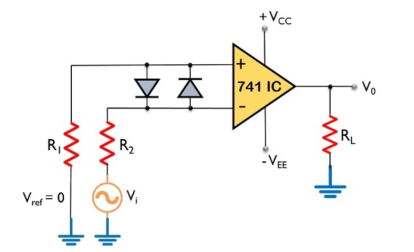
Fig 1 Zero crossing Detector
Here, the input signal Vi is provided to the inverting terminal of the op-amp while the non-inverting terminal is grounded by making use of two resistors R1 and R2.
It detects the point where the input signal crosses zero of the reference voltage level. For every crossing, the saturation level of the output signal changes from one to another.
The reference level is set at 0 and applied at the non-inverting terminal of the op-amp. The sine wave applied at the inverting terminal of the op-amp is compared with the reference level each time the phase of the wave changes either from positive to negative or negative to positive.
Firstly, when positive half of the sinusoidal signal appears at the input. Then the op-amp comparator compares the reference voltage level with the peak level of the applied signal.
Vo = Vref – Vi ---------------------------------------(1) And we know the reference level is 0, thus Vo = 0 – (+ Vsat) ----------------------------------------(2) Therefore, Vo = - Vsat ---------------------------------(3) During the negative half of the signal, thus the peak will have a negative polarity. Again Vo = Vref – Vi ---------------------------------------------(4) Thus, Vo = 0 - (- Vsat) --------------------------------------------------(5) So, we get Vo = + Vsat ---------------------------------------------(6) In this way, the zero -crossing detector detects the change in the level of the applied signal. |
Zero crossing detector is also known to be a square wave generator. As the output of the window comparator is nothing but a square wave.
|
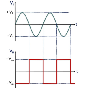
Fig 2 Input and output of zero crossing detector
V0 for the positive half of the applied signal is – Vsat,
This is the reason why we have achieved negative half of the square wave at the output when positive half of the sinusoidal signal is applied. While V0 for the negative half of the sinusoidal signal is + Vsat,
Applications:
- Phase Locked Loop
- Frequency counters and phase meters
Key takeaways
- An op-amp detector that has the ability to detect the change from positive to negative or negative to a positive level of a sinusoidal waveform is known as a zero- crossing detector.
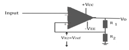
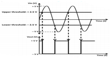
When comparator circuit used for zero crossing detector false triggering may takes place. The comparator circuit used to avoid such unwanted triggering is called regenerative comparator or Schmitt trigger. This basically uses positive feedback. The circuit diagram of basic Schmitt trigger is shown in figure. As the input is applied to inverting terminal it is an inverting Schmitt trigger. The inverting mode produces opposite polarity output. The output is fed back to the non-inverting input which is of same polarity as that of output, hence positive feedback.
CASE I: When Vin is slightly positive than Vref. The output gets driven in to negative saturation i.e. –Vsat level.
CASE II: When Vin is more negative than -Vref. The output gets driven in to positive saturation i.e. +Vsat level.
Thus, output voltage changes its state between +Vsat and –Vsat. Output voltage levels +Vsat and –Vsat are controlled by potential divider formed by R1.
|
Fig 3 Inverting Schmitt Trigger Circuit
|
Fig 4 Input and Output Waveform of Inverting Schmitt Trigger Circuit
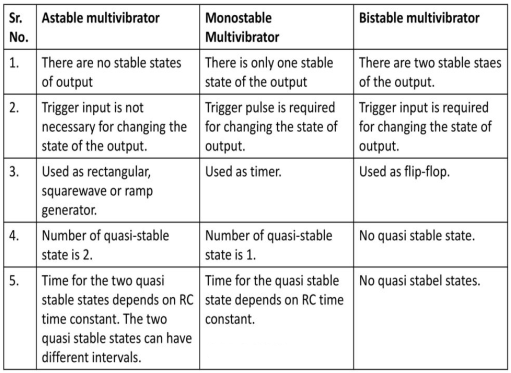
Astable mode
|
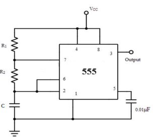
Fig 5 Astable Multivibrator
It is self-triggered multivibrator as pin 2 and 6 are connected. The supply is given through pin 8 and the output is obtained through pin 3. The timer will be reset if a low signal is given to pin 4. The capacitor is connected across pin 5 so that the external noise or any dc level are filtered. The resistor pair R1 and R2 form a circuit for determining the width of the output pulse.
|
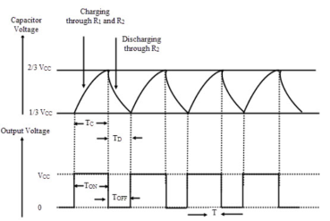
Fig 6 Capacitor and Output voltage waveform
During charging the capacitor charges through R1 and R2 and voltage across capacitor rises exponentially and during discharging the capacitor discharges through R2 and voltage falls exponentially. The output is obtained across pin 3.
The time for which capacitor charges from 1/3VCC to 2/3VCC is equal to the time the output is high which is given by tc= 0.69(R1+R2) C The discharging time from 2/3Vcc to 1/3VCC is given as td= 0.69 R2C The total period of output waveform is given by T = tc+ td = 0.69(R1+2R2) C The frequency of oscillations is given by f0 = The duty cycle is defined as the ratio of the charging time of capacitor at which the output is high to the total time period. %duty cycle = |
Applications of Astable Multivibrator
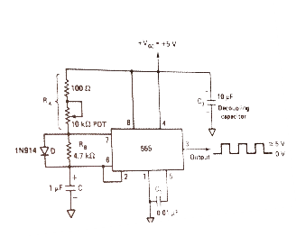
Square wave Oscillator: The astable multivibrator shown in the figure below [Ref.1] can be used to generate square wave oscillations. The diode is connected across RB and the diode and capacitor are charged through RA to a voltage of 2/3 of VCC. The capacitor discharges through RB and Q1. The discharging of capacitor when reaches 1/3VCC the discharging stops.
|
Fig 7 Astable multivibrator as square wave oscillator
Free-Running Ramp Generator
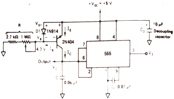
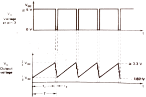
The circuit diagram is shown below [Ref.1]. The transistor Q1 is turned on by the comparator 1 when voltage across capacitor is 2/3Vcc. The capacitor C discharges through Q1. When capacitor discharges the voltage across C is 1/3Vcc, comparator 2 turns off Q1. The time period is given as
T = VCCC/3IC
|
Fig 7 Free Running Ramp generator circuit
|
Fig 8 Output waveform
IC = (VCC-VBE)/R
The free running frequency of ramp generator is given by
f0 = 3IC/VCCC
The output waveform is shown in above figure.
Mono-stable mode
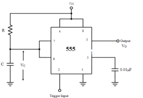
If the stable output is set at high (1), the output of the timer is high (1). At the application of an interrupt, the timer output turns low (0). Since the low state is unstable it goes to high (1) automatically after the interrupt passes. The monostable multivibrator using IC555 is shown below.
|
Fig 9 Monostable multivibrator using 555
The output is taken through pin 3. The supply is connected to pin 8. A small capacitor is connected to filter noise. The working is shown below in figure and explained as well.
|
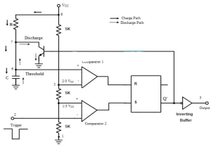
Fig 10 555 connected as monostable multivibrator
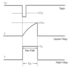
The discharge transistor will go to saturation when the F/F is reset. The discharge of C takes place through drain of CMOS. During negative pulse comparator 2 compares the pulse with reference voltage of 1/3 Vcc and output is low until the input becomes greater than the reference voltage. The output of F/F is set high when the output goes below 1/3Vcc. The output at pin 3 is high.
|
Fig 10 Input and Output waveform
When the C discharges the transistor is off and the voltage decays exponentially. This is input to the comparator 1 with reference voltage 2/3Vcc. The output is still high obtained at pin 3. The output of comparator is high when the threshold voltage becomes more than the reference voltage. Due to this the F/F is reset and output goes to zero. When the output is low the capacitor discharges completely and the transistor goes into saturation.
Pulse width
The voltage across C is Vc = Vcc (1-e-t/RC) When voltage across capacitor is 2/3Vcc 2/3Vcc = Vcc (1-e-t/RC) e-t/RC= 1/3 Taking log of both sides and solving we get t= 1.098RC The pulse width of rectangular pulse is 1.1RC (approx.) |
Application of Monostable Multivibrator
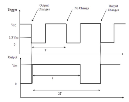
The monostable multivibrator can be used as frequency divider by adjusting the time interval off charging. The charging time is made larger than the period of input pulse the device acts as divide-by-2 network. By proper selection of R and C the timing interval can be controlled. The waveform is shown below.
|
Fig 12 Divide-by-2 circuit waveform
When negative input pulse is applied the output goes high and will remain high irrespective of any other input pulse application as the timing interval s greater than the time period of trigger pulse. The circuit is triggered for every alternate negative going pulse.
Pulse Stretcher
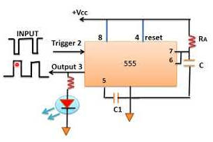
This application makes use of the fact that output pulse width of monostable multivibrator is larger than the negative pulse width of trigger pulse. The output of monostable multivibrator is the stretched form of the input pulse. The pulse stretcher is shown below.
|
Fig 13 Pulse Stretcher
Example-1
t1 – capacitor charge “ON” time is calculated as: t1 = 0.693(R1 + R2). C = 0.693(1000 +2000) x 10 x 10 -6 = 0.021 s= 0.21 msec t2 – capacitor discharge “OFF” time is calculated as: t2 = 0.693 R2. C = 0.693 X 2000 x 10 x 10 -6 = 14ms Total periodic time (T) is therefore calculated as: T = t1 + t2 = 21 ms + 14 ms = 35 ms. The output frequency, ƒ is therefore given as: f = 1/T = 1/35ms = 28.6 Hz Giving a duty cycle value of: Duty Cycle = R1 + R2 / (R1 + 2 R2) = 1000 + 2000/ (1000 + 2 x 2000) = 60% |
Key takeaways
|
First Order Active Low Pass Filter
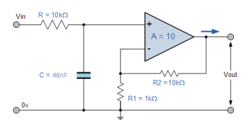
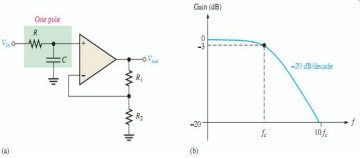
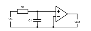
It is a simplistic filter that is composed of only one reactive component Capacitor accompanying with an active component Op-Amp. A resistor is utilized with the capacitor or inductor to form RC or RL low pass filter respectively. In a passive circuit, the output signal amplitude is smaller than the input signal amplitude. To surmount this problem, active circuit designs were introduced. When a passive low pass filter is connected to an Op-Amp either in inverting or non-inverting condition, it gives an active low pass filter design. The connection of a simple RC circuit with a single Op-Amp is shown in the image below.
|
Fig 14 First Order Active Low Pass Filter with the frequency response
This RC circuit assists in providing a low-frequency signal to the input of the amplifier. The amplifier operates as a unity gain output buffer circuit. This circuit has added input impedance value. The Op-Amp of the circuit has a very low output impedance value, which helps in providing high stability to the filter.
|
Fig 15 Active Low Pass Filter Circuit
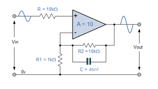
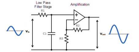
First Order Active Low Pass Filter with Amplification
|
Fig 16 Active Low Pass Filter with Amplification
In a non-inverting amplifier circuit configuration, the measurement of the voltage gain for the filter is given as a ratio of the feedback resistor (R2) divided by its corresponding input resistor (R3) value.

First Order Low Pass Filter Voltage Gain
The frequency components are used to obtain the voltage gain of the filter.
|
where,
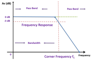
Vin is the input voltage When the frequency is increased, then the gain is decreased by 20 db. The operation of an active low pass filter can be checked from the above equation of frequency gain. Let f be the operating frequency and fc be the cutoff frequency. At low frequency When operating frequency is equal to cut off frequency And at high frequency From the above equations, it is seen that at low frequencies the gain of the circuit is equal to the maximum value of gain. Whereas at high frequencies condition, the gain of the circuit is very much lesser than the maximum gain Af. When the operating frequency is equal to cut off frequency, the gain is equal to 0.707 Af. In these filter circuits, the quantitative value (magnitude) of the passband gain is expressed in decibels or dB which is a function of the voltage gain.
|
|
Fig 17 Frequency Response Curve
Design:
Example-1
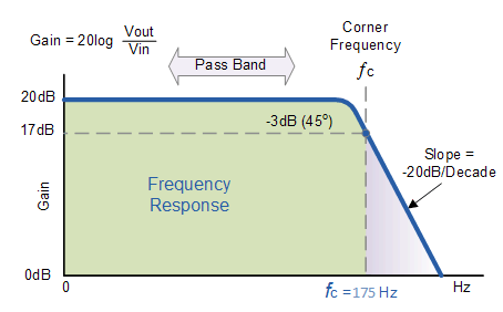
Design a non-inverting active low pass filter circuit that has a gain of ten at low frequencies, a high-frequency cut-off or corner frequency of 175Hz and an input impedance of 20KΩ. The voltage gain of the non-inverting amplifier is given as
Now assume the value of R1 to be 1KΩ and calculate the value R2 from the above equation.
Hence for a voltage gain of 10, values of R1 and R2 are 1KΩ and 9KΩ respectively. Gain in dB is given as 20LogA = 20Log10 = 20dB Now we are given with the cut-off frequency value as 175Hz and input impedance value as 20KΩ. By substituting these values in the equation and value of C can be calculated as follows.
|
Active Low Pass Filter Circuit
A typical circuit for an active low pass filter is given below:
|
Fig 18 Circuit design
Active Low Pass Filter Frequency Response Curve
The frequency response curve for an active low pass filter is given below:
|
Fig 19 Frequency Response of the problem
Non-Inverting Amplifier Filter
A simple non-inverting amplifier filter is given below:
|
Fig 20 Non-inverting circuit for the problem
Inverting Amplifier Filter
An equivalent inverting amplifier filter is given below:
|
Fig 21 Equivalent inverting circuit for the problem
Second Order Active Low Pass Filter
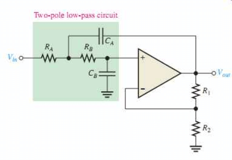
Second-Order Filters are also attributed to as VCVS filters since Op-Amp used here is Voltage Controlled Voltage Source Amplifier. This is another important type of active filter used in applications. The frequency response of the second-order low pass filter is indistinguishable to that of the first-order type besides that the stopband roll-off will be twice the first-order filters at 40dB/decade. Consequently, the design steps wanted of the second-order active low pass filter are identical. A simple method to get a second-order filter is to cascade two first-order filters.
|
Fig 22 Second-Order Active Low Pass Filter
Second Order Active Low Pass Filter Design and Example
Example-2
Assume Rs1 = Rs2 = 15KΩ and capacitor C1 = C2 = 100nF. The gain resistors are R1=1KΩ, R2= 9KΩ, R3 = 6KΩ, and R4 =3KΩ. Design a second-order active low pass filter with these specifications. The cut-off frequency is given as (1) The gain of first stage amplifier is The gain of second stage amplifier is Total Gain of the filter The total gain in dB (2) (3) The gain at cut-off frequency is (4)
|
Design and frequency scaling of First order and second order Active HP
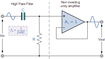
The basic operation of an Active High Pass Filter (HPF) is the same as for its equivalent RC passive high pass filter circuit, except this time the circuit has an operational amplifier or included within its design providing amplification and gain control.
First Order High Pass Filter
|
Fig 23 First Order HPF
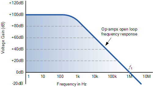
Frequency response curve of a typical Operational Amplifier
|
Fig 24 Frequency response curve of a typical Operational Amplifier
Then the performance of a “high pass filter” at high frequencies is limited by this unity gain crossover frequency which determines the overall bandwidth of the open-loop amplifier.
Example-3
Consider cut-off frequency value as 10 KHz, pass band gain Amax as 1.5 and capacitor value as 0.02 µF. The equation of the cut-off frequency is fC = 1 / (2πRC) By re-arranging this equation, we have R = 1 / (2πfC) R = 1/ (2π * 10000 * 0.02 * 10-6) = 795.77 Ω The pass band gain of the filter is Amax = 1 + (R3/R2) = 1.5 R3 = 0.5 R2 If we consider the R2 value as 10KΩ, then R3 = 5 kΩ We can calculate the gain of the filter as follows: Voltage Gain for High Pass filter: | Vout / Vin | = Amax * (f/fc) /√ [1 + (f/fc) ²] Av(dB) = 20 log10 (Vout/Vin) Second Order High Pass Filter Circuit |
The designing procedure for the second order active filter is same as that of the first order filter because the only variation is in the roll-off. If the roll-off of the first order active high pass filter is 20dB/decade, then roll-off of the second order filter is 40 dB/ decade. It means the twice of the value of the first order filter. The circuit of second order filter is shown below:
|
Fig 25 Second Order HPF
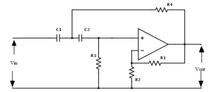
The gain of the filter is 1+ R1/R2 and the equation of the cut-off frequency is fc = 1/ 2π√R3R4C1C2. |
Second Order High Pass Filter Example
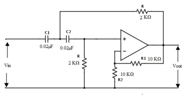
Design a filter with cut-off frequency 4 KHz and the delay rate in the stop band is 40dB/decade. As the delay rate in the stop band is 40dB/decade we can clearly say that the filter is second order filter.
Let us consider the capacitor values as C1= C2 = C = 0.02µF The equation of the cut-off frequency is fc = 1/ 2πRC Hz By re-arranging this equation we have R = 1/ 2πfC By substituting the values of cut-off frequency as 4 KHz and capacitor as 0.02µF R = 1.989 KΩ = 2KΩ. Let the gain of the filter is 1+ R1/R2 = 2 R1 / R2 = 1 R1 = R2 Therefore, we can take R1 = R2 = 10 KΩ |
Thus, the obtained filter is shown as below:
|
Fig 26 HPF Designed circuit
Key takeaways
- It can be used as a phase corrector.
- It is used to compensate the phase changes of voice signals that may have occurred over telephone wires during transmission.
- It is used in single side band suppressed carrier i.e. SSB-SC modulation based circuit designs.
1. Ramakant. A. Gayakwad, “Op-Amps & Linear Integrated Circuits”, 3rd Edition, PHI
2. S. Salivahanan & Bhaaskaran, “Linear Integrated Circuits”, 1st Edition, Tata McGraw Hill.
3. T.R Ganesh Babu, “Linear Integrated Circuits”, 3rd Edition, SciTech Publication
4. Sergio Franco, “Design with op-amp &Analog Integrated Circuits”, 3rd Edition, Tata McGraw Hill
5. “Operational Amplifiers and Linear IC’s”, David A. Bell, 2
nd edition, PHI/Pearson, 2004
6. “Linear Integrated Circuits”, D. Roy Choudhury and Shail B. Jain, 2nd edition, Reprint 2006, New Age International




![A_{v} (dB) = 20 log_{10}\left [ V_{out}/V_{in} \right ]](https://glossaread-contain.s3.ap-south-1.amazonaws.com/epub/1642935618_144696.png)
