UNIT 8
Other Linear IC applications
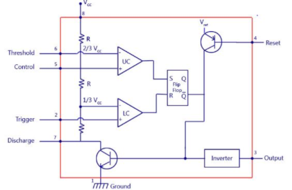
Fig 1 IC 555 Timer
For IC555 timer working as a flip flop or as a multi-vibrator, it has a particular set of configurations. Some of the major features include:
- It operates from a wide range of power ranging from +5 Volts to +18 Volts supply voltage.
- Sinking or sourcing 200 mA of load current.
- The external components should be selected properly so that the timing intervals can be made into several minutes along with the frequencies exceeding several hundred kilohertz.
- The output of a 555 timer can drive a transistor-transistor logic (TTL) due to its high current output.
- It has a temperature stability of 50 parts per million (ppm) per degree Celsius change in temperature which is equivalent to 0.005 %/ °C.
- The duty cycle of the timer is adjustable.
- Also, the maximum power dissipation per package is 600 mW and its trigger and reset inputs has logic compatibility.
Key takeaways
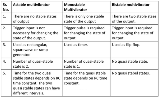
- They can be used as frequency divider, PWM, SR F/F, missing pulse detection etc.
The 555 generally operates in 3 modes:
- A-stable
- Mono-stable
- Bi-stable modes.
Astable mode
|
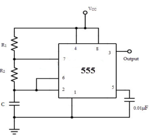
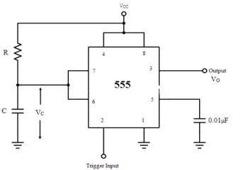
Fig 2 Astable Multivibrator
It is self-triggered multivibrator as pin 2 and 6 are connected. The supply is given through pin 8 and the output is obtained through pin 3. The timer will be reset if a low signal is given to pin 4. The capacitor is connected across pin 5 so that the external noise or any dc level are filtered. The resistor pair R1 and R2 form a circuit for determining the width of the output pulse.
|
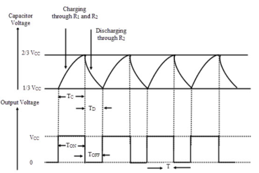
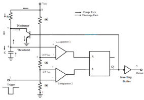
Fig 3 Capacitor and Output voltage waveform
During charging the capacitor charges through R1 and R2 and voltage across capacitor rises exponentially and during discharging the capacitor discharges through R2 and voltage falls exponentially. The output is obtained across pin 3.
The time for which capacitor charges from 1/3VCC to 2/3VCC is equal to the time the output is high which is given by tc= 0.69(R1+R2) C The discharging time from 2/3Vcc to 1/3VCC is given as td= 0.69 R2C The total period of output waveform is given by T = tc+ td = 0.69(R1+2R2) C The frequency of oscillations is given by f0 = The duty cycle is defined as the ratio of the charging time of capacitor at which the output is high to the total time period. %duty cycle = |
Applications of Astable Multivibrator
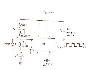
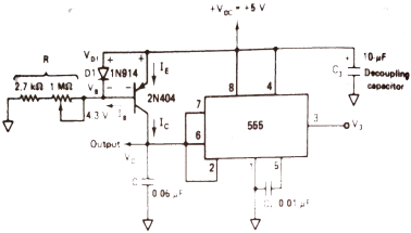
Square wave Oscillator: The astable multivibrator shown in the figure below [Ref.1] can be used to generate square wave oscillations. The diode is connected across RB and the diode and capacitor are charged through RA to a voltage of 2/3 of VCC. The capacitor discharges through RB and Q1. The discharging of capacitor when reaches 1/3VCC the discharging stops.
|
Fig 4 Astable multivibrator as square wave oscillator
Free-Running Ramp Generator
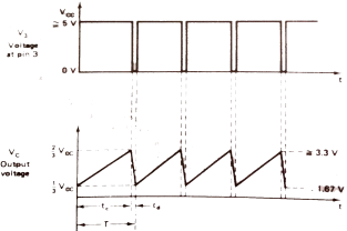
The circuit diagram is shown below [Ref.1]. The transistor Q1 is turned on by the comparator 1 when voltage across capacitor is 2/3Vcc. The capacitor C discharges through Q1. When capacitor discharges the voltage across C is 1/3Vcc, comparator 2 turns off Q1. The time period is given as
T = VCCC/3IC
|
Fig 5 Free Running Ramp generator circuit
|
Fig 6 Output waveform
IC = (VCC-VBE)/R The free running frequency of ramp generator is given by f0 = 3IC/VCCC The output waveform is shown in above figure. |
Mono-stable mode
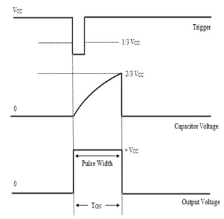
If the stable output is set at high (1), the output of the timer is high (1). At the application of an interrupt, the timer output turns low (0). Since the low state is unstable it goes to high (1) automatically after the interrupt passes. The monostable multivibrator using IC555 is shown below.
|
Fig 7 Monostable multivibrator using 555
The output is taken through pin 3. The supply is connected to pin 8. A small capacitor is connected to filter noise. The working is shown below in figure and explained as well.
|
Fig 8 555 connected as monostable multivibrator
The discharge transistor will go to saturation when the F/F is reset. The discharge of C takes place through drain of CMOS. During negative pulse comparator 2 compares the pulse with reference voltage of 1/3 Vcc and output is low until the input becomes greater than the reference voltage. The output of F/F is set high when the output goes below 1/3Vcc. The output at pin 3 is high.
|
Fig 9 Input and Output waveform
When the C discharges the transistor is off and the voltage decays exponentially. This is input to the comparator 1 with reference voltage 2/3Vcc. The output is still high obtained at pin 3. The output of comparator is high when the threshold voltage becomes more than the reference voltage. Due to this the F/F is reset and output goes to zero. When the output is low the capacitor discharges completely and the transistor goes into saturation.
Pulse width
The voltage across C is Vc = Vcc (1-e-t/RC) When voltage across capacitor is 2/3Vcc 2/3Vcc = Vcc (1-e-t/RC) e-t/RC= 1/3 Taking log of both sides and solving we get t= 1.098RC The pulse width of rectangular pulse is 1.1RC (approx..) |
Application of Monostable Multivibrator
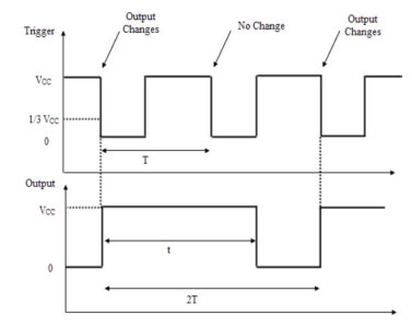
The monostable multivibrator can be used as frequency divider by adjusting the time interval off charging. The charging time is made larger than the period of input pulse the device acts as divide-by-2 network. By proper selection of R and C the timing interval can be controlled. The waveform is shown below.
|
Fig 10 Divide-by-2 circuit waveform
When negative input pulse is applied the output goes high and will remain high irrespective of any other input pulse application as the timing interval s greater than the time period of trigger pulse. The circuit is triggered for every alternate negative going pulse.
Pulse Stretcher
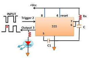
This application makes use of the fact that output pulse width of monostable multivibrator is larger than the negative pulse width of trigger pulse. The output of monostable multivibrator is the stretched form of the input pulse. The pulse stretcher is shown below.
|
Fig 11 Pulse Stretcher
Example-1
t1 – capacitor charge “ON” time is calculated as: t1 = 0.693(R1 + R2). C = 0.693(1000 +2000) x 10 x 10 -6 = 0.021 s= 0.21 msec t2 – capacitor discharge “OFF” time is calculated as: t2 = 0.693 R2. C = 0.693 X 2000 x 10 x 10 -6 = 14ms Total periodic time (T) is therefore calculated as: T = t1 + t2 = 21 ms + 14 ms = 35 ms. The output frequency, ƒ is therefore given as: f = 1/T = 1/35ms = 28.6 Hz Giving a duty cycle value of: Duty Cycle = R1 + R2 / (R1 + 2 R2) = 1000 + 2000/ (1000 + 2 x 2000) = 60%
|
Key takeaways
|
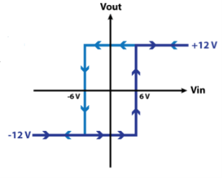
The Schmitt Trigger is a logic input type that provides hysteresis or two different threshold voltage levels for rising and falling edge. This is useful because it can avoid the errors when we have noisy input signals from which we want to get square wave signals.
Symmetrical
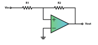
If we add a positive feedback by connecting the output voltage to the non-inverting input with a resistor between them and another resistor between the VIN and the non-inverting input we will get the Schmitt Trigger. Now the output will switch from VCC– to VCC+ when the voltage at the A node will cross 0 volts.
That means that now by adjusting the values of the resistors we can set at what value of the VIN input the switch will occur using the following equations. We get these equations with the following relationships. The current “i” through this line equals VIN – VA divided by R1 as well as VA – VOUT divided by R2. So if we replace the VA with zero, as we need that value for the switch to occur, we will get that final equation.
|
Fig 20 Symmetrical

Va = 0


|
Fig 21 Symmetrical characteristics
Asymmetrical
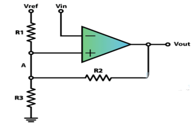
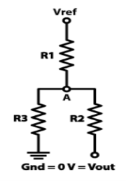
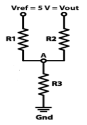
In order to get two different non-symmetrical thresholds, we can use this circuit of an inverting single powered Schmitt Trigger. Here the VREF voltage is the same as the VCC of the op-amp. Now because the VIN input is connected to the inverting input of the op-amp when its values will reach the upper threshold, the output will switch off to 0 volts, and then when its values will decline to the lower threshold, the output will switch on to 5 volts.
|
Fig 22 Asymmetrical
Example-1
|
|
Vout = 0V

Va = 166V
Vout = 5V

Va = 333V
Key takeaway
- The Schmitt Trigger is a logic input type that provides hysteresis or two different threshold voltage levels for rising and falling edge. This is useful because it can avoid the errors when we have noisy input signals from which we want to get square wave signals.
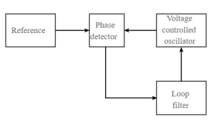
A phase-locked loop consists of a phase detector and a voltage-controlled oscillator. The output of the phase detector is the input of the voltage-controlled oscillator (VCO) and the output of the VCO is connected to one of the inputs of a phase detector which is shown below in the basic block diagram. When these two devices are feed to each other the loop forms.
A basic phase locked loop, PLL, consists of three basic elements:
|
Fig 13 Block Diagram of PLL
- Phase comparator / detector: As the name implies, this circuit block within the PLL compares the phase of two signals and generates a voltage according to the phase difference between the two signals.
- Voltage controlled oscillator, VCO: The voltage-controlled oscillator is the circuit block that generates the radio frequency signal that is normally considered as the output of the loop. Its frequency can be controlled over the operational frequency band required for the loop.
- Loop filter: This filter is used to filter the output from the phase comparator in the phase locked loop, PLL. It is used to remove any components of the signals of which the phase is being compared from the VCO line, i.e. the reference and VCO input. It also governs many of the characteristics of the loop including the loop stability, speed of lock, etc.
Operation
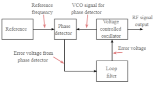
- The diagram for a basic phase locked loop shows the three main element of the PLL: phase detector, voltage- controlled oscillator and the loop filter.
- In the basic PLL, reference signal and the signal from the voltage- controlled oscillator are connected to the two input ports of the phase detector.
- The output from the phase detector is passed to the loop filter and then filtered signal is applied to the voltage- controlled oscillator.
- The Voltage Controlled Oscillator, VCO, within the PLL produces a signal which enters the phase detector. The phase of the signals from the VCO and the incoming reference signal are compared and a resulting difference or error voltage is produced. This corresponds to the phase difference between the two signals.
- The error signal from the phase detector passes through a low pass filter which governs many of the properties of the loop and removes any high frequency elements on the signal.
- Once through the filter the error signal is applied to the control terminal of the VCO as its tuning voltage. The sense of any change in this voltage is such that it tries to reduce the phase difference and hence the frequency between the two signals.
- Initially the loop will be out of lock, and the error voltage will pull the frequency of the VCO towards that of the reference, until it cannot reduce the error any further and the loop is locked.
- When the PLL, phase locked loop, is in lock a steady state error voltage is produced. By using an amplifier between the phase detector and the VCO, the actual error between the signals can be reduced to very small levels.
- However, some voltage must always be present at the control terminal of the VCO as this is what puts onto the correct frequency.
|
Fig 14 PLL showing voltages
The fact that a steady error voltage is present means that the phase difference between the reference signal and the VCO is not changing. As the phase between these two signals is not changing means that the two signals are on exactly the same frequency.
Key takeaways
- The phase locked loop has three main elements: phase detector, voltage- controlled oscillator and the loop filter. When the PLL, phase locked loop, is in lock a steady state error voltage is produced. By using an amplifier between the phase detector and the VCO, the actual error between the signals can be reduced to very small levels.
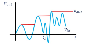
Peak detector circuits are used to determine the peak (maximum) value of an input signal. It stores the peak value of input voltages for infinite time duration until it comes to reset condition. The peak detector circuit utilizes its property of following the highest value of an input signal and storing it.
Rectifier circuits usually provide an output in proportion to the average value of the input. However, some application requires measurement of the peak value of the signal. Thus, peak detectors are used. Usually, the peak of non-sinusoidal waveforms is measured using a peak detector.
|
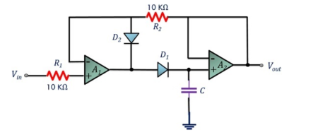
Fig 15 Peak detector
The peak of the input waveform is followed and stored in terms of voltage in the capacitor. If the circuit detects a higher peak, the new peak value is stored in the capacitor until it is discharged.
The capacitor employed in the circuit is charged through the diode by the applied input signal. The small voltage drop across the diode is ignored and the capacitor is charged up to the highest peak of the applied input signal.
Let us consider initially the capacitor is charged to voltage Vc. The diode employed in the circuit gets forward biased when the applied input voltage Vin exceeds the capacitor voltage Vc. Thereby allowing the circuit to behave as a voltage follower. The output voltage follows the applied input voltage until Vin is more than Vc.
As the input voltage Vin reduces below the value of capacitive voltage Vc, it causes the diode to get reverse biased. In such condition, the capacitor retains the value until the input again exceeds the value stored in the capacitor.
|
Fig 16 Wave form of output
The basic circuit of the peak detector contains only one Op-amp. A high impedance load is offered by the op-amp A1 to the source. While op-amp A2 performs buffering action in between the load and capacitor.
To prevent the effect of the offset voltage, the value of the two resistances R1 and R2 are kept equal.
The necessary frequency compensation must be given to op-amp A1 in order to have stability against oscillations.
Applications of Peak detector
- It is used in the analysis of spectral and mass spectrometer.
- Peak detector finds its application in destructive testing.
- It is used for instrumentation measurement, mostly in amplitude modulated wave communication.
- It widely finds applications in sound measuring instruments.
|
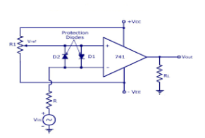
Fig17 Comparator
- A reference voltage Vref of 1V is applied to the inverting terminal of op-amp.
- A time varying voltage Vin is applied to the non-inverting terminal of op-amp.
- Diode D1 and D2 are used to protect the op-amp from damage from excess amount of input voltage Vin.
- They are known as clamp diodes as they clamp the difference input voltage to +0.7V to -0.7V.
- Hence, the above circuit is called as non-inverting Comparator.
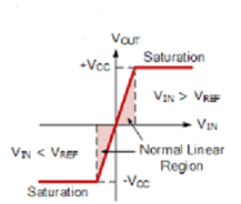
Characteristics of comparator
|
Fig 18 Voltage levels for comparator
|
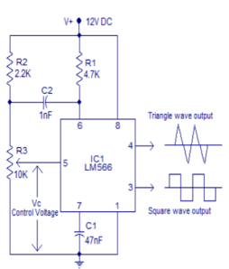
These oscillators are the one whose output frequency can be varied by varying the amplitude of input voltage signal. It is also known as voltage to frequency converter. The block diagram is shown below. The resistor R1 and capacitor C1 determines the frequency of oscillations. Through terminal 5 Vc is applied. As the capacitor charges by current source and linearly discharges through external capacitor triangular wave is generated.
|
Fig 19 VCO using 566
The charge discharge action is provided by Schmitt trigger action. The square wave output is due to the Schmitt trigger. Resistor R1 and capacitor C1 form the timing components. Capacitor C2 is used to prevent the parasitic oscillations during VCO switching. Resistor R3 is used to provide the control voltage Vc. Triangle and square wave outputs are obtained from pins 4 and 3 respectively.
Key takeaways
- It is also known as voltage to frequency converter. These oscillators are the one whose output frequency can be varied by varying the amplitude of input voltage signal.
D/ A converters
Resistor weighted and R-2R DAC
Weighted Resistor DAC
A weighted resistor DAC produces an analog output, which is almost equal to the digital (binary) input by using binary weighted resistors in the inverting adder circuit. In short, a binary weighted resistor DAC is called as weighted resistor DAC.
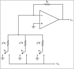
The circuit diagram of a 3-bit binary weighted resistor DAC is shown in the following figure −
|
Fig 20 DAC
The bits of a binary number can have only one of the two values. i.e., either 0 or 1. Let the 3-bit binary input is b2b1b0. Here, the bits b2 and b0 denote the Most Significant Bit (MSB) and Least Significant Bit (LSB) respectively.
The digital switches shown in the above figure will be connected to ground, when the corresponding input bits are equal to ‘0’
Similarly, the digital switches shown in the above figure will be connected to the negative reference voltage, −VR when the corresponding input bits are equal to ‘1’.
In the above circuit, the non-inverting input terminal of an op-amp is connected to ground. That means zero volts is applied at the non-inverting input terminal of op-amp.
According to the virtual short concept, the voltage at the inverting input terminal of opamp is same as that of the voltage present at its non-inverting input terminal. So, the voltage at the inverting input terminal’s node will be zero volts.
The nodal equation at the inverting input terminal’s node is: (0 + VR b2) / 2 0 R + 0 + VR b1 / 2 1 R + 0 + VR b0 / 2 2 R + 0 -V0 /Rf =0 Vo /Rf = VR b2 / 2 0 R + VR b1 / 2 1 R + VR b0 / 2 2 R Vo = VR .Rf/ R { b2 / 2 0 + b1 / 2 1 + b0 / 2 2 } Substituting R = 2Rf in the above equation Vo = VR . Rf / 2 Rf { b2 / 2 0 + b1 / 2 1 + b0 / 2 2 } Vo = VR / 2 { b2 / 2 0 + b1 / 2 1 + b0 / 2 2 } |
The above equation represents the output voltage equation of a 3-bit binary weighted resistor DAC. Since the number of bits are three in the binary (digital) input, we will get seven possible values of output voltage by varying the binary input from 000 to 111 for a fixed reference voltage, VR.
We can write the generalized output voltage equation of an N-bit binary weighted resistor DAC as shown below based on the output voltage equation of a 3-bit binary weighted resistor DAC.
=>V0=VR/2{bN−1/20+bN−2/21+....+b0/2N−1} |
The disadvantages of a binary weighted resistor DAC are as follows −
- The difference between the resistance values corresponding to LSB & MSB will increase as the number of bits present in the digital input increases.
- It is difficult to design more accurate resistors as the number of bits present in the digital input increases.
R-2R Ladder DAC
The R-2R Ladder DAC overcomes the disadvantages of a binary weighted resistor DAC. As the name suggests, R-2R Ladder DAC produces an analog output, which is almost equal to the digital (binary) input by using a R-2R ladder network in the inverting adder circuit.
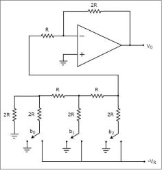
The circuit diagram of a 3-bit R-2R Ladder DAC is shown in the following figure
|
Fig 21 R-2R Ladder
Let the 3-bit binary input is b2b1b0. Here, the bits b2 and b0 denote the Most Significant Bit (MSB) and Least Significant Bit (LSB) respectively.
The digital switches shown in the above figure will be connected to ground, when the corresponding input bits are equal to ‘0’. Similarly, the digital switches shown in above figure will be connected to the negative reference voltage, −VR when the corresponding input bits are equal to ‘1’.
It is difficult to get the generalized output voltage equation of a R-2R Ladder DAC. But, we can find the analog output voltage values of R-2R Ladder DAC for individual binary input combinations easily.
The advantages of a R-2R Ladder DAC are as follows −
- R-2R Ladder DAC contains only two values of resistor: R and 2R. So, it is easy to select and design more accurate resistors.
- If more number of bits are present in the digital input, then we have to include required number of R-2R sections additionally.
SAR
|
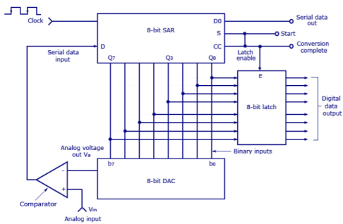
Fig 23 SAR
- The main part of the circuit is the 8-bit SAR, whose output is given to an 8-bit D/A converter.
- The analog output Va of the D/A converter is then compared to an analog signal Vin by the comparator.
- The output of the comparator is a serial data input to the SAR. Till the digital output (8 bits) of the SAR is equivalent to the analog input Vin, the SAR adjusts itself.
- The 8-bit latch at the end of conversation holds onto the resultant digital data output.
- At the start of a conversion cycle, the SAR is reset by making the start signal (S) high.
- The MSB of the SAR (Q7) is set as soon as the first transition from LOW to HIGH is introduced.
- The output is given to the D/A converter which produces an analog equivalent of the MSB and is compared with the analog input Vin.
- If comparator output is LOW, D/A output will be greater than Vin and the MSB will be cleared by the SAR.
If comparator output is HIGH, D/A output will be less than Vin and the MSB will be set to the next position (Q7 to Q6) by the SAR. - According to the comparator output, the SAR will either keep or reset the Q6 bit. This process goes on until all the bits are tried.
- After Q0 is tried, the SAR makes the conversion complete (CC) signal HIGH to show that the parallel output lines contain valid data. The CC signal in turn enables the latch, and digital data appear at the output of the latch.
- As the SAR determines each bit, digital data is also available serially. As shown in the figure above, the CC signal is connected to the start conversion input in order to convert the cycle continuously.
- The biggest advantage of such a circuit is its high speed. It may be more complex than an A/D converter, but it offers better resolution.
A/ D converters
Analog to digital converter samples the analog signal on each falling or rising edge of sample clock. In each cycle, the ADC gets of the analog signal, measures and converts it into a digital value. The ADC converts the output data into a series of digital values by approximates the signal with fixed precision.
In ADCs, two factors determine the accuracy of the digital value that captures the original analog signal. These are quantization level or bit rate and sampling rate.
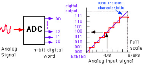
The figure depicts how analog to digital conversion takes place. Bit rate decides the resolution of digitized output
The figure displays 3-bit ADC is used for converting analog signal.
|
Fig 24 ADC
Assume that one volt signal has to be converted from digital by using 3-bit ADC as shown below. Therefore, a total of 2^3=8 divisions are available for producing 1V output. This results 1/8=0.125V is called as minimum change or quantization level represented for each division as 000 for 0V, 001 for 0.125, and likewise upto 111 for 1V. If we increase the bit rates like 6, 8, 12, 14, 16, etc. we will get a better precision of the signal. Thus, bit rate or quantization gives the smallest output change in the analog signal value that results from a change in the digital representation.
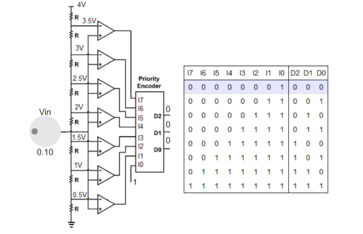
Flash ADC
- Flash analog-to-digital converters, also known as parallel ADCs, are the fastest way to convert an analog signal to a digital signal.
- Flash ADCs are ideal for applications requiring very large bandwidth, but they consume more power and much bigger in size than other ADC architectures.
- A Flash converter requires a huge number of comparators compared to other ADCs, especially as the resolution increases.
- A Flash converter requires 2n-1 comparators for an n-bit conversion.
|
Fig 25 Flash generator
- Circuit shown is a 3- bit flash converter
- Reference ladder consists of 2n (23 = 8) equal size resistors
- Input voltage is compared to 2n-1 reference voltages using 2n-1 comparator. The reference voltages can be calculated using KVL.
- A Priority Encoder is used to transform the comparator outputs to the correct digital binary output.
- Change the input voltage and observe the comparators and the priority encoder digital outputs.
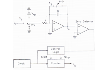
Dual slope ADC
|
Fig 26 Dual Slope ADC
Working:
- At t<0, S1 is set to ground , S2 is closed and counter =0.
- At t=0 conversion begins and S2 is open and S1 is set so the input to the integrator is Vin.
- Si is held for T INT which is a constant predetermined time interval.
- When S1 is set the counter begins to count clock pulses, the counter resets to zero after TINT
- Vout of integrator at t=TINT is Vin TINT /RC linearly proportional to Vin.
- At t= TINT S1 is set so -Vref is the input to the integrator which has the volatage VIN TINT /RC stored in it.
- The integrator voltage then drops linearly with a slope -Vref/RC
- The comparator is used to determine when the output voltage of the integrator crosses zero
- When it is zero the digitized output value is the state of the counter.
Key takeaways
- The difference between the resistance values corresponding to LSB & MSB will increase as the number of bits present in the digital input increases.
- It is difficult to design more accurate resistors as the number of bits present in the digital input increases.
References:
1. Ramakant. A. Gayakwad, “Op-Amps & Linear Integrated Circuits”, 3rd Edition, PHI
2. S.Salivahanan&Bhaaskaran, “Linear Integrated Circuits”, 1st Edition, Tata McGraw Hill.
3. T.R Ganesh Babu, “Linear Integrated Circuits”, 3rd Edition, SciTech Publication
4. Sergio Franco, “Design with op-amp &Analog Integrated Circuits”, 3rd Edition, Tata McGraw Hill
5. “Operational Amplifiers and Linear IC’s”, David A. Bell, 2
nd edition, PHI/Pearson, 2004
6. “Linear Integrated Circuits”, D. Roy Choudhury and Shail B. Jain, 2nd edition, Reprint 2006, New Age International
