Unit-1
Microprocessors and Microcontrollers
A microcontroller is a chip optimized to control electronic devices. It is stored in a single integrated circuit which is dedicated for performing task and execute a specific application.
A microprocessor is a controlling unit of a micro-computer wrapped inside a small chip. It performs Arithmetic Logical Unit (ALU) operations and communicates with the other devices connected with it. It is a single Integrated Circuit in which several functions are combined.
Microprocessor | Microcontroller |
Microprocessor is the heart of the Computer System | Microcontroller is the heart of the embedded system |
It is just a processor. Memory and I/O components have to be connected externally | Microcontroller has external processor along with internal memory and I/O components |
Since memory and I/O has to be connected externally the circuit becomes large | Since memory and I/O are present internally the circuit is small. |
Cannot be used in compact systems hence inefficient | Can be used in compact systems and hence it is an efficient technique |
Cost of the entire system increases | Cost of the entire system is low |
Do not have power saving features | Have power modes like idle mode and power saving mode |
Microprocessors has less number of registers | Microcontrollers have more number of registers. |
Key Take Aways:
Microprocessor consists of only a Central Processing Unit, whereas Micro Controller contains a CPU, Memory, I/O all integrated into one chip
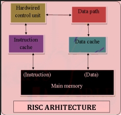
RISC is reduced instruction set computer which uses simple commands that can be divided into several instructions to achieve low-level operation within a single CLK. The CPU design plan is based on simple orders and acts fast. The pipelining technique is crucial technique used to speed up RISC machines.
|
Figure 1. RISC Architecture
The features of RISC include the following
- The demand of decoding is less
- Few data types in hardware
- General purpose register Identical
- Uniform instruction set
- Simple addressing nodes
Also, while writing a program, RISC makes it easier by letting the computer programmer to eliminate needless codes and stops wasting of cycles.
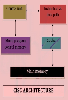
CISC is complex instruction set computer is computer where single instructions can perform numerous low-level operations like load from memory, an arithmetic operation, and memory store or are accomplished by multi-step processes or addressing modes in single instructions
It is a CPU design plan based on single commands, which are skilled in executing multi-step operations.
CISC computers have small programs. It has a huge number of compound instructions, which takes a long time to perform. Here, a single set of instruction is protected in several steps; each instruction set has additional than 300 separate instructions. Maximum instructions are finished in two to ten machine cycles. In CISC, instruction pipelining is not easily implemented.
|
Figure 2. CISC Architecture
Key Take Aways:
CISC has the ability to execute addressing modes or multi-step operations within one instruction set.
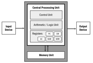
Von-Neumann architecture In Von-Neumann architecture, the same memory and bus are used to store both data and instructions that run the program. Since it is not possible to access program memory and data memory simultaneously, the Von Neumann architecture is susceptible to bottlenecks and system performance is affected
|
Figure 3. Von-Neumann architecture
Harvard Architecture The Harvard architecture stores machine instructions and data in separate memory units that are connected by different busses. In this case, there are at least two memory address spaces to work with, so there is a memory register for machine instructions and another memory register for data. Computers designed with the Harvard architecture are able to run a program and access data independently, and therefore simultaneously. Harvard architecture has a strict separation between data and code. Thus, Harvard architecture is more complicated but separate pipelines remove the bottleneck that Von Neumann creates.
|
Figure 4: The Harvard architecture has a separate bus for signals and storage.
Key Takeaways:
The Harvard architecture stores machine instructions and data in separate memory units that are connected by different busses
Computer software is programming code executed on a computer processor. The code can be machine-level code, or code written for an operating system.
An operating system is software intended to provide a predictable and dependable layer for other programmers to build other software on, which are known as applications.
It also provides a dependable layer for hardware manufacturers. This standardization creates an efficient environment for programmers to create smaller programs, which can be run by millions of computers. Software can also be thought of as an expression that contrasts with hardware.
The physical components of a computer are the hardware; the digital programs running on the hardware are the software. Software can also be updated or replaced much easier than hardware. Basically, software is the computer logic computer users interact with.
Key Take Aways:
Software, instructions that tell a computer what to do. Software comprises the entire set of programs, procedures, and routines associated with the operation of a computer system.
1.5.1 Introduction
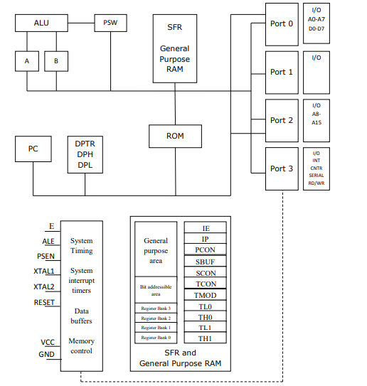
8051 microcontrollers was designed by Intel in 1981. It is an 8-bit microcontroller built with 40 pins DIP (dual inline package), 4kb of ROM storage and 128 bytes of RAM storage, 2 16-bit timers.
It consists of are four parallel 8-bit ports, which are programmable as well as addressable as per the requirement. An on-chip crystal oscillator is integrated in the microcontroller having crystal frequency of 12 MHz
1.5.2 Architecture of 8051
|
Figure 5. 8051 architecture.
- 8051 microcontroller was designed by Intel in 1981.
- It is an 8-bit microcontroller.
- It is built with 40 pins DIP (dual inline package), 4kb of ROM storage and 128 bytes of RAM storage, 2 16-bit timers.
- It consists of are four parallel 8-bit ports, which are programmable as well as addressable depending on the requirement.
- An on-chip crystal oscillator is integrated in the microcontroller having crystal frequency of 12 MHz.
- 8051 has 4 K Bytes of internal ROM. The address space is from 0000 to 0FFFh. If the program size is more than 4 K Bytes 8051 will fetch the code automatically from external memory.
- Accumulator is an 8 bit register widely used for all arithmetic and logical operations. Accumulator is also used to transfer data between external memory. B register is used along with Accumulator for multiplication and division. A and B registers together is also called MATH registers.
- PSW (Program Status Word). This is an 8 bit register which contains the arithmetic status of ALU and the bank select bits of register banks
CY | AC | F0 | RS1 | RS0 | OV | - | P |
CY - carry flag
AC - auxiliary carry flag
F0 - available to the user for general purpose.
RS1,RS0 – register bank select bits.
OV – overflow
P – parity
1.5.3 Pin Diagram of 8051
Figure 6. Pin Diagram of 8051
Pin out Description:
Pin 1-8 | PORT1- Each of these pins can be configured as an input or output. |
Pin 9 | RESET- A logic set on this pin disables the microcontroller and clears the contents of most registers. In other words a positive voltage on this pin resets the microcontroller. |
Pin 10-17 | PORT -3: Similar to Port 1.Each pin serves as general output or input .Besides all of them have alternate functions. |
Pin 10 RXD | Serial Asynchronous Communication Input or Serial Synchronous Communication Output. |
Pin 11 TXD | Serial Asynchronous Communication Output or Serial Synchronous Communication clock output |
Pin 12 INT0 | External Interrupt 0 input |
Pin 14 INT1 | External Interrupt 1 input |
Pin 15 T0 | T0 Counter 0 clock input |
Pin16 T1 | T1 Counter 1 clock input |
Pin 17 RD | Read from external RAM |
Pin 18, 19 XTAL2, XTAL1 | Internal oscillator input and output. A quartz crystal which specifies operating frequency is usually connected to these pins. |
Pin 20 GND | Ground |
Pin 21-28 Port 2 | If there is no intention to use external memory then these port pins are configured as general inputs/outputs. In case external memory is used, the higher address byte, i.e. addresses A8-A15 will appear on this port. Even though memory with capacity of 64Kb is not used, which means that not all eight port bits are used for its addressing, the rest of them are not available as inputs/outputs. |
Pin 29 PSEN | If external ROM is used for storing program then a logic zero (0) appears on it every time the microcontroller reads a byte from memory. |
Pin 30 ALE | Prior to reading from external memory, the microcontroller puts the lower address byte (A0-A7) on P0 and then activates the ALE output. After receiving signal from ALE pin, the external latch latches the state of P0 and uses it as a memory chip address. Immediately the ALE pin is returned to its previous logic state and P0 is now used as a Data Bus. |
Pin 31 EA | By applying logic zero to this pin, P2 and P3 are used for data and address transmission whether there is internal memory or not. It means that even if there is a program written to the microcontroller, it will not be executed. Instead, the program written to external ROM and executed. By applying logic one to the EA pin, the microcontroller will use both memories, first internal then external if present. |
Pin 32-39 PORT 0 | Similar to P2, if external memory is not used, these pins can be used as general inputs/outputs. Otherwise, P0 is configured as address output (A0-A7) when the ALE pin is driven high (1) or as data output (Data Bus) when the ALE pin is driven low (0). |
Pin 40 VCC | +5V power supply |
8051 microcontrollers has 4 I/O ports each of 8-bit, which can be configured as input or output. Hence, total 32 input/output pins allow the microcontroller to be connected with the peripheral devices.
Pin configuration, i.e. the pin can be configured as 1 for input and 0 for output as per the logic state.
Input/Output (I/O) pin − All the circuits within the microcontroller must be connected to one of its pins except P0 port because it does not have pull-up resistors built-in.
1.5.4 Memory Organization
The 8051 Microcontroller Memory is separated into Program Memory (ROM) and Data Memory (RAM). The Program Memory of the 8051 Microcontroller is used for storing the program to be executed, which means instructions. The Data Memory is used for storing temporary variable data and intermediate results.
8051 Microcontroller has both Internal ROM and Internal RAM. If the internal memory is inadequate, you can add external memory using suitable circuits.
Program Memory (ROM) of 8051
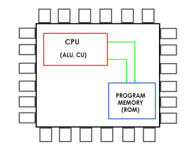
In 8051 Microcontroller, the code or instructions that has to be executed are stored in the Program Memory, which is also called as the ROM of the Microcontroller. The original 8051 Microcontroller by Intel has 4KB of internal ROM.
|
Figure 7. Program Memory
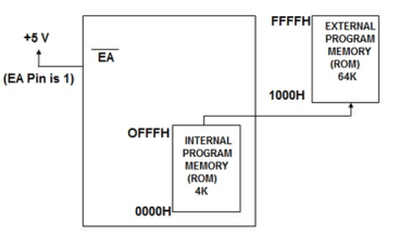
In 4KB of Internal ROM, the address space is 0000H to 0FFFH. If the address space that is the program addresses exceeds this value, then the CPU will automatically fetch the code from the external Program Memory.
For External Access Pin (EA Pin) must be pulled HIGH i.e. when the EA Pin is high, the CPU first fetches instructions from the Internal Program Memory in the address range of 0000H to 0FFFFH and if the memory addresses exceed the limit, then the instructions are fetched from the external ROM in the address range of 1000H to FFFFH.
|
Figure 8. External Access
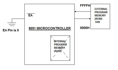
There is also an alternative method to fetch the instructions that is ignore the Internal ROM and fetch all the instructions only from External Program Memory(External ROM).
For this purpose EA pin must be connected to GND . In this case the memory addresses of external ROM will be from 0000H to FFFFH.
|
Figure 9. EA pin ground
Data Memory (RAM) of 8051 Microcontroller
Data Memory or RAM of 8051 Microcontroller stores temporary data and intermediate results that are generated and used during the normal operation of the microcontroller. Original Intel’s 8051 Microcontroller had 128B of internal RAM.
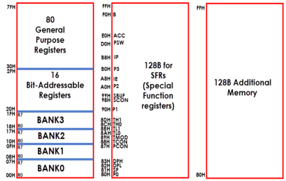
Currently 8051 Microcontroller have 256B of RAM. Of this 256B, the first 128B memory addresses from 00H to 7FH is divided in to Working Registers organized as Register Banks, Bit – Addressable Area and General Purpose RAM known as Scratchpad area.
In the first 128B of RAM (from 00H to 7FH), the first 32B that is memory from addresses 00H to 1FH consists of 32 Working Registers that are organized as four banks with 8 Registers in each Bank.
|
Lower 128B(00H to 07H) Upper 128B(80H-FFH)
(Direct and Indirect Addressing) (Direct Addressing) (Indirect Addressing)
Figure 10 . Register Bank
The 4 banks are named as Bank0, Bank1, Bank2 and Bank3. Each Bank consists of 8 registers named as R0 – R7. Each Register can be addressed in two ways: by name or by address.
To address the register by name, first the corresponding Bank has to be selected. In order to select the bank, use RS0 and RS1 bits of the Program Status Word (PSW) Register (RS0 and RS1 are 3rd and 4th bits in the PSW Register).
When addressing the Register using its address say 12H for example, the corresponding Bank may or may not be selected. (12H corresponds to R2 in Bank2).
The next 16B of the RAM i.e. from 20H to 2FH are Bit – Addressable memory locations. There are totally 128 bits that can be addressed individually using 00H to 7FH or the entire byte can be addressed as 20H to 2FH.
The final 80B of the internal RAM addresses from 30H to 7FH, is the general purpose RAM area which are byte addressable.
These lower 128B of RAM can be addressed directly or indirectly.
SRFs Memory addresses are only direct addressable. Even though some of the addresses between 80H and FFH are not assigned to any SFR, they cannot be used as additional RAM area.
In some microcontrollers, there is an additional 128B of RAM, which share the memory address with SFRs that is 80H to FFH. But, this additional RAM block is only accessed by indirect addressing.
1.5.5 External Memory Interfacing
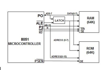
The design for 8051 Microcontroller based system is not limited to the internal RAM and ROM present in the 8051 Microcontroller. There is also a provision of connecting both external RAM and ROM that is Data Memory and Program.
The reason for interfacing external Program Memory or ROM is that complex programs written in high – level languages often tend to be larger and occupy more memory.
Another important reason is that chips like 8031 or 8032, do not have any internal ROM but must be interfaced with external ROM.
A maximum of 64B of Program Memory (ROM) and Data Memory (RAM) each can be interfaced with the 8051 Microcontroller.
Consider the following block diagram of interfacing 64KB of External RAM and 64KB of External ROM with the 8051 Microcontroller.
|
Figure 11. External Memory Interfacing
1.5.6 Stacks
The stack is a section of a RAM used by the CPU to store information such as data or memory address on temporary basis. The CPU needs this storage area considering limited number of registers.
In the 8051, the stack pointer (SP) points to the last used location of the stack. When data is pushed onto the stack, the stack pointer (SP) is incremented by 1. When PUSH is executed, the contents of the register are saved on the stack and SP is incremented by 1. To push the registers onto the stack, we must use their RAM addresses. For example, the instruction "PUSH 1" pushes register R1 onto the stack.
Popping the contents of the stack back into a given register is the opposite to the process of pushing. With every pop operation, the top byte of the stack is copied to the register specified by the instruction and the stack pointer is decremented once.
Key Takeaways:
8051 microcontrollers is designed by Intel in 1981. It is an 8-bit microcontroller. It is built with 40 pins DIP (dual inline package), 4kb of ROM storage and 128 bytes of RAM storage, 2 16-bit timers. It consists of are four parallel 8-bit ports, which are programmable as well as addressable as per the requirement. An on-chip crystal oscillator is integrated in the microcontroller having crystal frequency of 12 MHz.
References:
- The 8051 Microcontroller and Embedded Systems using Assembly and C by Muhammad Ali Mazidi.
- The 8051 Microcontroller by I. Scott Mackenzie, Raphael C.W Phan
3. 8051 Microcontrollers: Internals, Instructions, Programming, and Interfacing Book by Subrata Ghoshal
