Unit-7
Motivation for MSP430 Microcontrollers
7.1.1 Low Power Embedded Systems
The features of the MSP430 make it ideal for battery powered measurement applications. The MSP430 architecture is designed specifically for ultra low power devices. Specific operating modeare implemented to reduce power consumption and extend battery life. Other important low power features, such as zero power brownout reset and extremely low pin leakage, have enabled MSP430 customers to develop battery based products which last for over 10 years from its original battery.
7.1.2 On-chip Peripherals
On–chip Peripherals (analog and digital):
Memory: These devices have flash memory, up to 512KB and RAM up to 66KB.
Digital I/O Ports: MSP430x5xx devices may have up to 12 digital I/O ports implemented, P1 to P11 and PJ. Most ports have eight I/O pins, however some ports may contain less. Each I/O pin is individually configurable for input or output direction, and each I/O line can be individually read or written to.
All ports have individually configurable pullup or pulldown resistors. Ports P1 and P2 always have interrupt capability. Port pairs P1/P2, P3/P4, P5/P6, P7/P8, etc. are associated with the names PA, PB, PC, PD, etc., respectively.
The digital I/O features include:
• Independently programmable individual I/Os
• Any combination of input or output
• Individually configurable P1 and P2 interrupts
• Independent input and output data registers
• Individually configurable pullup or pulldown resistors
7.1.3 Low Power RF capabilities
MSP430 devices control all of the settings of the RF device through simple universal digital interface and process and generate the received or transmitted data. The MSP430 can switch the TRF6900 into standby/shutdown mode to reduce power consumption, while consuming virtually no power of its own.
In addition to the core performance, devices in the family are available with a range of integrated peripheral options, including a 14-bit analog to digital converter (ADC), liquid crystal display (LCD) driver, universal synchronous asynchronous receiver transmitter (USART) and several different timer configurations.
7.1.3 Target applications:
7.1.3.1 Single-chip
Single-chip solution in place of multi-chip
• Interfaces to a variety of current sensors
• Support for various wired/wireless protocols
• Metrology engine in Hardware/Software
|
Figure1. On-chip solutions
7.1.3.2 Low Cost and Low Power
The MSP430 Microcontroller Value Line brings 16-bit performance, up to 16MHz operation, integrated intelligent peripherals, and ultra-low power at low-cost 8-bit MCU prices for cost sensitive applications.
Features:
- Up to 16MHz CPU speed
- 1.8V - 3.6V operation
- Up to 56kB Flash
- Up to 4KB RAM
- MSP430G2xx2, G2xx3, and G2xx5 devices provide unique capacitive touch sense IO ports.
- As low as(@2.2V): 0.1μA RAM retention
- 0.4μA Standby mode (VLO)
- 0.7μA real-time clock mode
- 220μA/MHz active
- Ultra-Fast Wake-Up From Standby Mode in <1μs
7.1.3.4 High Performance System Design
MSP430F563x and MSP430F663x families add performance and features to its ultra low power 16-bit microcontroller portfolio. Developers take advantage of the microcontrollers' larger memory, display capacity and analog peripherals, which enable high precision measurement and connectivity.
The F563x and F663x devices meet the needs of portable measurement applications, including blood glucose meters, pulse oximeters, blood pressure monitors, electrocardiograms (ECG), activity monitors and sensor hubs. Home automation and industrial applications requiring a user interface such as utility meters, remote sensing and thermostats also benefit from the ultra-low-power, high-performance capabilities of these MSP430 families.
Key Takeaway:
Home automation and industrial applications requiring a user interface such as utility meters, remote sensing and thermostats also benefit from the ultra-low-power, high-performance capabilities of these MSP430 families.
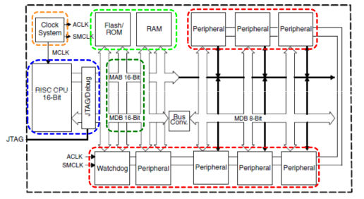
|
Figure 2. Architecture
Features:
- Efficient ultra- low power CPU
- C-compiler friendly
- RISC architecture
- -27 core instructions
- -24 emulated instructions
- -7 addressing modes
- Constant generator
- Single cycle register operations
- Memory-to-memory atomic addressing
- Bit, Byte and Word Processing
- 20-bit addressing on MSP430 for flash > 64kB
Key Takeaways:
Texas Instruments MSP430™ Family of Ultra-Low Power Microcontrollers (MCUs) includes several devices featuring different sets of peripherals for various applications.
7.2.1 Instruction set
* ADC[.W] Add carry to destination
* ADC.B Add carry to destination
Syntax
ADC dst or ADC.W dst ADC.B dst
Operation
dst + C → dst
Emulation
ADDC #0,dst
ADDC.B #0,dst
Description
The carry bit (C) is added to the destination operand. The previous contents of the destination are lost
Example
The 8-bit counter pointed to by R13 is added to a 16-bit counter pointed to by R12.
ADD.B @R13,0(R12) ; Add LSDs
ADC.B 1(R12) ; Add carry to MSD
2. ADD
ADD[.W] Add source word to destination word
ADD.B Add source byte to destination byte
Syntax
ADD src,dst or ADD.W src,dst
ADD.B src,dst Operation src + dst → dst
Description
The source operand is added to the destination operand. The previous content of the destination is lost.
3. ADDC
ADDC[.W] Add source word and carry to destination word
ADDC.B Add source byte and carry to destination byte
Syntax
ADDC src,dst or ADDC.W src,dst
ADDC.B src,dst
Operation src + dst + C → dst
Description:
The source operand and the carry bit C are added to the destination operand. The previous content of the destination is lost.
4. AND
AND[.W] Logical AND of source word with destination word
AND.B Logical AND of source byte with destination byte
Syntax AND src,dst or AND.W src,dst
AND.B src,dst Operation src .and. dst → dst
Description
The source operand and the destination operand are logically ANDed. The result is placed into the destination. The source operand is not affected.
Example
AND.B @R5+,R6 ; AND table byte with R6. R5 + 1
5. BIC
BIC[.W] Clear bits set in source word in destination word
BIC.B Clear bits set in source byte in destination byte
Syntax
BIC src,dst or BIC.W src,dst
BIC.B src,dst
Operation (.not. src) .and. dst → dst
Description The inverted source operand and the destination operand are logically ANDed. The result is placed into the destination. The source operand is not affected.
6.BIS
BIS[.W] Set bits set in source word in destination word
BIS.B Set bits set in source byte in destination byte
Syntax
BIS src,dst or BIS.W src,dst
BIS.B src,dst
Operation src .or. dst → dst
Description The source operand and the destination operand are logically ORed. The result is placed into the destination. The source operand is not affected.
Example:
Bits 15 and 13 of R5 (16-bit data) are set to one. R5.19:16 = 0
BIS #A000h,R5 ; Set R5 bits
7. BIT
BIT[.W] Test bits set in source word in destination word
BIT.B Test bits set in source byte in destination byte
Syntax BIT src,dst or BIT.W src,dst BIT.B src,dst
Operation src .and. dst
Description The source operand and the destination operand are logically ANDed. The result affects only the status bits in SR
* BR, Branch to destination in lower 64K address space
BRANCH
Syntax BR dst
Operation dst → PC
Emulation MOV dst,PC
Description An unconditional branch is taken to an address anywhere in the lower 64K address space. All source addressing modes can be used. The branch instruction is a word instruction.
Example
BR @R5+ ; Branch to the address contained in the word pointed ; to by R5 and increment pointer in R5 afterwards. ; The next time-S/W flow uses R5 pointer-it can ; alter program execution due to access to ; next address in a table pointed to by R5 ; Core instruction MOV @R5,PC ; Indirect, indirect R5 with autoincrement
CALL
CALL Call a subroutine in lower 64 K
Syntax CALL dst
Operation dst → tmp 16-bit dst is evaluated and stored
SP – 2 → SP
PC → @SP updated PC with return address to TOS
tmp → PC saved 16-bit dst to PC
Description A subroutine call is made from an address in the lower 64 K to a subroutine address in the lower 64 K. All seven source addressing modes can be used. The call instruction is a word instruction. The return is made with the RET instruction.
CLR
* CLR[.W] Clear destination
* CLR.B Clear destination
Syntax
CLR dst or CLR.W dst
CLR.B dst
Operation 0 → dst
Emulation
MOV #0,dst
MOV.B #0,dst
Description The destination operand is cleared.
CLRC
* CLRC Clear carry bit
Syntax
CLRC Operation 0 → C
Emulation BIC #1,SR
Description The carry bit (C) is cleared. The clear carry instruction is a word instruction.
CLRN
* CLRN Clear negative bit
Syntax CLRN
Operation 0 → N or (.NOT.src .AND. dst → dst)
Emulation BIC #4,SR
Description The constant 04h is inverted (0FFFBh) and is logically ANDed with the destination operand. The result is placed into the destination. The clear negative bit instruction is a word instruction.
CLRZ
* CLRZ Clear zero bit
Syntax CLRZ
Operation 0 → Z or (.NOT.src .AND. dst → dst)
Emulation BIC #2,SR
Description The constant 02h is inverted (0FFFDh) and logically ANDed with the destination operand. The result is placed into the destination. The clear zero bit instruction is a word instruction
CMP
CMP[.W] Compare source word and destination word
CMP.B Compare source byte and destination byte
Syntax CMP src,dst or CMP.W src,dst CMP.B src,dst
Operation (.not.src) + 1 + dst or dst – src
Emulation BIC #2,SR
Description The source operand is subtracted from the destination operand. This is made by adding the 1s complement of the source + 1 to the destination. The result affects only the status bits in SR. Register mode: the register bits Rdst.19:16 (.W) resp. Rdst. 19:8 (.B) are not cleared.
DADC
* DADC[.W] Add carry decimally to destination
* DADC.B Add carry decimally to destination
Syntax DADC dst or DADC.W dst
DADC.B dst
Operation dst + C → dst (decimally) Emulation DADD #0,dst DADD.B #0,dst Description The carry bit (C) is added decimally to the destination.
DADC
* DADC[.W] Add carry decimally to destination
* DADC.B Add carry decimally to destination
Syntax DADC dst or DADC.W dst
DADC.B dst
Operation dst + C → dst (decimally)
Emulation DADD #0,dst DADD.B #0,dst
Description The carry bit (C) is added decimally to the destination.
DEC
* DEC[.W] Decrement destination
* DEC.B Decrement destination
Syntax DEC dst or
DEC.W dst DEC.B dst
Operation dst – 1 → dst
Emulation SUB #1,dst SUB.B #1,dst
Description The destination operand is decremented by one. The original contents are lost.
DECD
* DECD[.W] Double-decrement destination
* DECD.B Double-decrement destination
Syntax DECD dst or
DECD.W dst DECD.B dst
Operation dst – 2 → dst
Emulation SUB #2,dst SUB.B #2,dst
Description The destination operand is decremented by two. The original contents are lost.
DINT
* DINT Disable (general) interrupts
Syntax DINT
Operation 0 → GIE or
(0FFF7h .AND. SR → SR / .NOT.src .AND. dst → dst)
Emulation BIC #8,SR
Description All interrupts are disabled. The constant 08h is inverted and logically ANDed with the SR. The result is placed into the SR.
INV
* INV[.W] Invert destination
* INV.B Invert destination
Syntax INV dst or
INV.W dst INV.B dst
Operation .not.dst → dst
Emulation XOR #0FFFFh,dst XOR.B #0FFh,dst
Description The destination operand is inverted. The original contents are lost.
JC Jump if carry
JHS Jump if higher or same (unsigned)
Syntax
JC label
JHS label
Operation
If C = 1: PC + (2 × Offset) → PC
If C = 0: execute the following instruction
Description The carry bit C in the SR is tested. If it is set, the signed 10-bit word offset contained in the instruction is multiplied by two, sign extended, and added to the 20-bit PC. This means a jump in the range –511 to +512 words relative to the PC in the full memory range. If C is reset, the instruction after the jump is executed. JC is used for the test of the carry bit C. JHS is used for the comparison of unsigned numbers.
JEQ, JZ
JEQ Jump if equal
JZ Jump if zero
Syntax
JEQ label
JZ label
Operation
If Z = 1: PC + (2 × Offset) → PC If Z = 0: execute following instruction
Description The zero bit Z in the SR is tested. If it is set, the signed 10-bit word offset contained in the instruction is multiplied by two, sign extended, and added to the 20-bit PC. This means a jump in the range –511 to +512 words relative to the PC in the full memory range. If Z is reset, the instruction after the jump is executed. JZ is used for the test of the zero bit Z. JEQ is used for the comparison of operands.
JGE Jump if greater or equal (signed)
Syntax
JGE label
Operation
If (N .xor. V) = 0: PC + (2 × Offset) → PC
If (N .xor. V) = 1: execute following instruction
Description The negative bit N and the overflow bit V in the SR are tested. If both bits are set or both are reset, the signed 10-bit word offset contained in the instruction is multiplied by two, sign extended, and added to the 20-bit PC. This means a jump in the range -511 to +512 words relative to the PC in full Memory range.
If only one bit is set, the instruction after the jump is executed. JGE is used for the comparison of signed operands: also for incorrect results due to overflow, the decision made by the JGE instruction is correct.
Note that JGE emulates the non-implemented JP (jump if positive) instruction if used after the instructions AND, BIT, RRA, SXTX, and TST. These instructions clear the V bit.
JL
JL Jump if less (signed)
Syntax JL label
Operation If (N .xor. V) = 1: PC + (2 × Offset) → PC
If (N .xor. V) = 0: execute following instruction
Description The negative bit N and the overflow bit V in the SR are tested. If only one is set, the signed 10-bit word offset contained in the instruction is multiplied by two, sign extended, and added to the 20-bit PC. This means a jump in the range –511 to +512 words relative to the PC in full memory range. If both bits N and V are set or both are reset, the instruction after the jump is executed. JL is used for the comparison of signed operands: also for incorrect results due to overflow, the decision made by the JL instruction is correct.
JMP
JMP Jump unconditionally
Syntax JMP label
Operation PC + (2 × Offset) → PC
Description The signed 10-bit word offset contained in the instruction is multiplied by two, sign extended, and added to the 20-bit PC. This means an unconditional jump in the range –511 to +512 words relative to the PC in the full memory. The JMP instruction may be used as a BR or BRA instruction within its limited range relative to the PC.
JN
JN Jump if negative
Syntax JN label
Operation
If N = 1: PC + (2 × Offset) → PC
If N = 0: execute following instruction
Description The negative bit N in the SR is tested. If it is set, the signed 10-bit word offset contained in the instruction is multiplied by two, sign extended, and added to the 20-bit program PC. This means a jump in the range -511 to +512 words relative to the PC in the full memory range. If N is reset, the instruction after the jump is executed.
JNC, JLO
JNC Jump if no carry
JLO Jump if lower (unsigned)
Syntax
JNC label JLO label
Operation If C = 0: PC + (2 × Offset) → PC If C = 1: execute following instruction
Description The carry bit C in the SR is tested. If it is reset, the signed 10-bit word offset contained in the instruction is multiplied by two, sign extended, and added to the 20-bit PC. This means a jump in the range –511 to +512 words relative to the PC in the full memory range. If C is set, the instruction after the jump is executed. JNC is used for the test of the carry bit C. JLO is used for the comparison of unsigned numbers.
JNZ, JNE
JNZ Jump if not zero
JNE Jump if not equal
Syntax JNZ label
JNE label
Operation If Z = 0: PC + (2 × Offset) → PC
If Z = 1: execute following instruction
Description The zero bit Z in the SR is tested. If it is reset, the signed 10-bit word offset contained in the instruction is multiplied by two, sign extended, and added to the 20-bit PC. This means a jump in the range –511 to +512 words relative to the PC in the full memory range. If Z is set, the instruction after the jump is executed. JNZ is used for the test of the zero bit Z. JNE is used for the comparison of operands.
MOV
MOV[.W] Move source word to destination word
MOV.B Move source byte to destination byte
Syntax
MOV src,dst or MOV.W src,dst
MOV.B src,dst
Operation src → dst
Description The source operand is copied to the destination. The source operand is not affected.
NOP
* NOP No operation
Syntax NOP Operation None
Emulation MOV #0, R3
Description No operation is performed. The instruction may be used for the elimination of instructions during the software check or for defined waiting times. Status Bits Status bits are not affected.
POP
* POP[.W] Pop word from stack to destination
* POP.B Pop byte from stack to destination
Syntax POP dst POP.B dst
Operation @SP → temp SP + 2 → SP temp → dst
Emulation
MOV @SP+,dst or MOV.W @SP+,dst
MOV.B @SP+,dst
Description The stack location pointed to by the SP (TOS) is moved to the destination. The SP is incremented by two afterwards.
Status Bits Status bits are not affected.
PUSH
PUSH[.W] Save a word on the stack
PUSH.B Save a byte on the stack
Syntax
PUSH dst or PUSH.W dst
PUSH.B dst
Operation SP – 2 → SP dst → @SP
Description The 20-bit SP SP is decremented by two. The operand is then copied to the RAM word addressed by the SP. A pushed byte is stored in the low byte; the high byte is not affected.
RET
* RET Return from subroutine
Syntax RET
Operation @SP →PC.15:0 Saved PC to PC.15:0. PC.19:16 ← 0 SP + 2 → SP Description
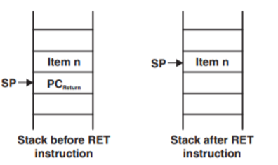
The 16-bit return address (lower 64 K), pushed onto the stack by a CALL instruction is restored to the PC. The program continues at the address following the subroutine call. The four MSBs of the PC.19:16 are cleared.
Example
Call a subroutine SUBR in the lower 64 K and return to the address in the lower 64 K after the CALL. CALL #SUBR ; Call subroutine starting at SUBR ... ;
Return by RET to here
SUBR PUSH R14 ; Save R14 (16 bit data) ... ;
Subroutine code POP R14 ;
POP R14 Restore R14
RET Return to lower 64K
|
Figure 3. Stack after RET instruction
RETI
RETI Return from interrupt
Syntax
RETI
Operation
@SP → SR.15:0 Restore saved SR with PC.19:16
SP + 2 → SP @SP → PC.15:0 Restore saved
PC.15:0 SP + 2 → SP Housekeeping
Description The SR is restored to the value at the beginning of the interrupt service routine. This includes the four MSBs of the PC.19:16. The SP is incremented by two afterward. The 20-bit PC is restored from PC.19:16 (from same stack location as the status bits) and PC.15:0.
The 20-bit PC is restored to the value at the beginning of the interrupt service routine. The program continues at the address following the last executed instruction when the interrupt was granted. The SP is incremented by two afterward.
RLA
* RLA[.W] Rotate left arithmetically
* RLA.B Rotate left arithmetically
Syntax RLA dst or RLA.W dst RLA.B dst
Operation C ← MSB ← MSB-1 .... LSB+1 ← LSB ← 0
Emulation ADD dst,dst ADD.B dst,dst
Description The destination operand is shifted left one position as shown in Figure . The MSB is shifted into the carry bit (C) and the LSB is filled with 0. The RLA instruction acts as a signed multiplication by 2. An overflow occurs if dst ≥ 04000h and dst < 0C000h before operation is performed; the result has changed sign.
|
Figure 4. Arithmetic shift left
* RLC[.W] Rotate left through carry
* RLC.B Rotate left through carry
Syntax RLC dst or RLC.W dst RLC.B dst
Operation C ← MSB ← MSB-1 .... LSB+1 ← LSB ← C
Emulation ADDC dst,dst
Description The destination operand is shifted left one position as shown in Figure. The carry bit (C) is shifted into the LSB, and the MSB is shifted into the carry bit (C).
|
Figure 5.Carry left Shift
RRA
RRA[.W] Rotate right arithmetically destination word
RRA.B Rotate right arithmetically destination byte
Syntax RRA.B dst or RRA.W dst
Operation MSB → MSB → MSB–1 → ... LSB+1 → LSB → C
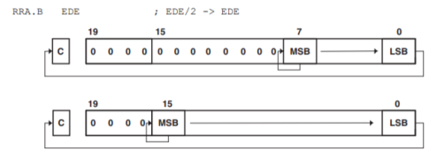
Description The destination operand is shifted right arithmetically by one bit position as shown in Figure. The MSB retains its value (sign).
RRA operates equal to a signed division by 2. The MSB is retained and shifted into the MSB–1. The LSB+1 is shifted into the LSB. The previous LSB is shifted into the carry bit C.
|
Figure 6. Rotate Right Arithmetically RRA.B and RRA.W
RRC
RRC[.W] Rotate right through carry destination word
RRC.B Rotate right through carry destination byte
Syntax RRC dst or RRC.W dst RRC.B dst
Operation C → MSB → MSB–1 → ... LSB+1 → LSB → C
Description The destination operand is shifted right by one bit position as shown in Figure. The carry bit C is shifted into the MSB and the LSB is shifted into the carry bit C.
SETC ; Prepare carry for MSB
RRC EDE ; EDE = EDE >> 1 + 8000h
|
Figure 7. Rotate Right Through Carry RRC.B and RRC.W
* SBC[.W]
Subtract borrow (.NOT. carry) from destination
* SBC.B
Subtract borrow (.NOT. carry) from destination
Syntax
SBC dst or SBC.W dst SBC.B dst
Operation dst + 0FFFFh + C → dst dst + 0FFh + C → dst
Emulation SUBC #0,dst SUBC.B #0,dst
Description The carry bit (C) is added to the destination operand minus one. The previous contents of the destination are lost.
Example
The 16-bit counter pointed to by R13 is subtracted from a 32-bit counter pointed to by R12.
SUB @R13,0(R12) ; Subtract LSDs
SBC 2(R12) ; Subtract carry from MSD
SUB
SUB[.W] Subtract source word from destination word
SUB.B Subtract source byte from destination byte
Syntax
SUB src,dst or SUB.W src,dst
SUB.B src,dst
Operation
(.not.src) + 1 + dst → dst or dst – src → dst
Description The source operand is subtracted from the destination operand. This is made by adding the 1s complement of the source + 1 to the destination. The source operand is not affected, the result is written to the destination operand.
Example
A 16-bit constant 7654h is subtracted from RAM word EDE.
SUB #7654h,&EDE ; Subtract 7654h from EDE
SUBC
SUBC[.W] Subtract source word with carry from destination word
SUBC.B Subtract source byte with carry from destination byte
Syntax
SUBC src,dst or SUBC.W src,dst
SUBC.B src,dst
Operation (.not.src) + C + dst → dst or dst – (src – 1) + C → dst
Description The source operand is subtracted from the destination operand. This is done by adding the 1s complement of the source + carry to the destination. The source operand is not affected, the result is written to the destination operand. Used for 32, 48, and 64-bit operands.
Example
A 16-bit constant 7654h is subtracted from R5 with the carry from the previous instruction.
R5.19:16 = 0
SUBC.W #7654h,R5 ;
Subtract 7654h + C from R5
SWPB
SWPB Swap bytes
Syntax SWPB dst
Operation dst.15:8 ↔ dst.7:0
Description The high and the low byte of the operand are exchanged. PC.19:16 bits are cleared in register mode.
Example
Exchange the bytes of RAM word EDE (lower 64 K)
MOV #1234h,&EDE ; 1234h -> EDE
SWPB &EDE ; 3412h -> EDE
|
Figure8. Swap bytes in memory.
|
Figure9. Swap bytes in register
SXT
SXT Extend sign
Syntax SXT dst
Operation dst.7 → dst.15:8,
dst.7 → dst.19:8 (register mode)
Description
Register mode: the sign of the low byte of the operand is extended into the bits Rdst.19:8.
Rdst.7 = 0: Rdst.19:8 = 000h
afterwards
Rdst.7 = 1: Rdst.19:8 = FFFh afterwards
Other modes: the sign of the low byte of the operand is extended into the high byte.
dst.7 = 0: high byte = 00h afterward
s dst.7 = 1: high byte = FFh afterwards
Example
The signed 8-bit data in EDE (lower 64 K) is sign extended and added to the 16-bit signed data in R7. MOV.B &EDE,R5 ; EDE -> R5.
00XXh SXT R5 ; Sign extend low byte to R5.19:8
ADD R5,R7 ; Add signed 16-bit values
XOR
XOR[.W] Exclusive OR source word with destination word
XOR.B Exclusive OR source byte with destination byte
Syntax XOR src,dst or XOR.W src,dst XOR.B src,dst
Operation src .xor. dst → dst
Description The source and destination operands are exclusively ORed. The result is placed into the destination. The source operand is not affected. The previous content of the destination is lost.
Key Take Aways:
The core instructions have unique op-codes decoded by the CPU, while the emulated ones need assemblers and compilers to generate their mnemonics.
7.2.2 Clock system
The clock system on the MSP430 is designed to be flexible and low power.
The MSP has three clock sources for the clocking system, and three clock lines that chip systems can choose between. The clock sources are used as the basis for the clock lines, and this allows for a mix of slow and fast clocks to be used around the system. The three clock sources are:
- Low Frequency Crystal Clock (LFXTCLK) – this signal is meant to come from a watch crystal external to the MSP itself. The crystal connects to the XIN and XOUT pins, and the intended oscillation is 32kHz. This is the source of the Auxiliary Clock line (ACLK). The primary control of this source is that it can be turned off with the OSCOFF option in the Status Register. The source also has a high-speed mode for faster crystals.
- Crystal 2 Clock (XT2CLK) – this signal is the second external clock source, and it is connected to the XT2IN and XT2OUT pins. In general, this signal is meant to be the high-speed clock source.
- Digitally Controlled Oscillator Clock (DCOCLK) – this is the only internally generated clock input, and it is the default clock source for the master clock upon reset. By default this clock runs at about 900kHZ, but the RSELx, MODx, and DCOx bits allow this to be divided down or even blended to achieve a lower clock frequency on average.
The three clock lines are:
- Master Clock (MCLK) – This clock is the source for the MSP CPU core; this clock must be working properly for the processor to execute instructions. This clock has the most selection for its source. The source is selected with the SELMx bits of the Basic Clock System Control Register 2 (BCSCTL2). The divider is controlled with the DIVMx of the BCSCTL2. Finally, the CPU can be turned off with the CPUOFF bit of the Status Register (SR), but to recover from this state an interrupt must occur.
- Submaster Clock (SMCLK) - This clock is the source for most peripherals, and its source can either be the DCO or Crystal 2. The source clock is controlled with the SELS and SCG bits of the BCSCTL2 and SR. The divider is controlled by the DIVSx bits of the BCSCTL2.
- Auxiliary Clock (ACLK) - this clock line’s source is always LFXTCLK. It is an option for slower subsystems to use to conserve power. This clock can be divided as controlled by the DIVAx bits of the Basic Clock System Control Register 1 (BCSCTL1).
The MSP clock system has dividers at the beginning of its clocks, and at most peripheral destinations.
Key Take Aways:
The MSP has three clock sources for the clocking system, and three clock lines that chip systems can choose.
7.2.3 Memory Subsystem
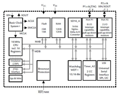
The main blocks are linked by the memory address bus (MAB) and memory data bus (MDB).
-The MSP430 has flash memory of 2KB, and 128 bytes of RAM.
-Six blocks are shown for peripheral functions include
1. Port P1: 8 input/output pins with interrupt capability,
2. Port P2: 2 input/output pins with interrupt capability,
3. 16-Bit Timer_A with Two Capture/Compare Registers,
4. A watchdog timer.
5. The universal serial interface (USI)
6. 16-Bit sigma–delta analog-to-digital converter (SD16_A)
-The brownout protection comes into action if the supply voltage drops to a dangerous level.
-There are ground and power supply connections. Ground is labeled VSS and is taken to define 0V. The supply connection is VCC.
|
Figure 10. Memory in MSP430
Key Takeaways:
The MSP430 family's memory space is configured in a "von-Neumann Architecture" and has code memory (ROM, EPROM, RAM) and data memory (RAM, EEPROM, ROM) in one address space using a unique address and data bus.
7.3.1 Understanding how to use CCS for Assembly
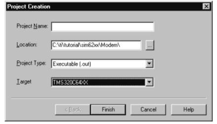
The information for a project is stored in a single project file (*.pjt). The following procedure to create new projects, one at a time. When multiple projects are created, each project’s filename must be unique . Step 1: From the Project menu, choose New. The Project Creation wizard window displays. Figure 11. Project Creation Step 2: In the Project Name field, type the name for the project. Each project you create must have a unique name. Step 3: In the Location field, specify directory to store the project file. Type the full path in the Location field or click the Browse button and use the Choose Directory dialog box. Step 4: In the Project Type field, select a Project Type from the drop-down list. Choose either Executable (.out) or Library (lib). Executable indicates that the project generates an executable file. Library indicates that you are building an object library. Step 5: In the Target field, select the Target Family that identifies the CPU. This information is necessary when tools are installed for multiple targets. Step 6: Click Finish. After creating a new project file, add the filenames of the source code, object libraries, and linker command file to the project list.
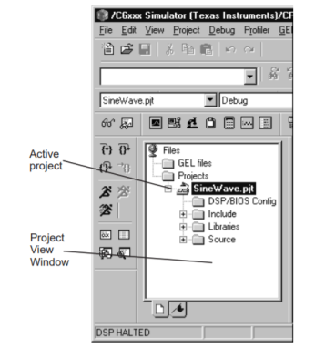
Figure 12. Code Composer Studio Project Management and Editing Tools
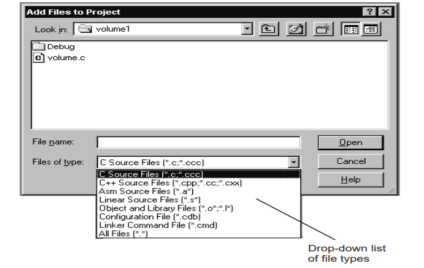
Adding Files to a Project Step 1: Select Project→Add Files to Project, or or right-click on the project’s filename in the Project View window and select Add Files. The Add Files to Project dialog box displays.
Figure 13. Adding files
Step 2: In the Add Files to Project dialog box, specify a file to add. If the file does not exist in the current directory, browse to the correct location. Use the Files of type drop-down list to set the type of files that appear in the File name field. Step 3: Click Open to add the specified file to your project. The Project View is automatically updated when a file is added to the current project.
Figure14 . Selection Building and Running the Program To build and run a program, follow these steps Step 1: Choose Project→Rebuild All or click the (Rebuild All) toolbar button. The CCS IDE recompiles, reassembles, and relinks all the files in your project. Messages about this process are shown in a frame at the bottom of the window. Step 2: By default, the .out file is built into a debug directory located under your current project folder. To change this location, select a different one from the CCS toolbar.
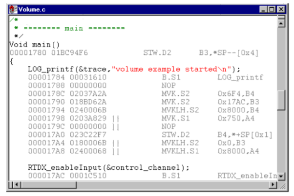
Figure 15. Selection Step 3: Choose File→Load Program. Select the program you just rebuilt, and click Open. The CCS IDE loads the program onto the target DSP and opens a Dis-Assembly window that shows the disassembled instructions that make up the program. (Notice that the CCS IDE also automatically opens a tabbed area at the bottom of the window to show the output that the program sends to stdout.) Step 4: Choose View→Mixed Source/ASM. This allows you to simultaneously view your c source and the resulting assembly code . Step 5: Click on an assembly instruction in the mixed-mode window. (Click on the actual instruction, not the address of the instruction or the fields passed to the instruction.) Press the F1 key. The CCS IDE searches for help on that instruction. This is a good way to get help on an unfamiliar assembly instruction. Building and Running the Program Code Composer Studio Project Management and Editing Tools . Step 6: Choose Debug→Go Main to begin execution from the main function. The execution halts at main and is identified by . Step 7: Choose Debug→Run or click the (Run) toolbar button to run the program. Step 8: Choose Debug→Halt to quit running the program.
|
Key Differentiating factors between different MSP430 families
- Complete system on-a-chip — includes LCD control, ADC, I/O ports, ROM, RAM, basic timer, watchdog timer, UART, etc.
- Extremely low power consumption — only 4.2 nW per instruction, typical High speed — 300 ns per instruction @ 3.3 MHz clock, in register and register addressing mode RISC structure — 27 core instructions
- Orthogonal architecture (any instruction with any addressing mode)
- Seven addressing modes for the source operand Four addressing modes for the destination operand Constant generator for the most often used constants (–1, 0, 1, 2, 4, 8)
- Only one external crystal required — a frequency locked loop (FLL) oscillator derives all intern
7.3.2 C
Code Composer Studio allows you to edit C and assembly source code. You can also view C source code with the corresponding assembly instructions shown after the C statements.
|
Figure 16. Editor
The integrated editor provides support for the following activities:
❏ Highlighting of keywords, comments, and strings in color
❏ Marking C blocks in parentheses and braces, finding matching or next parenthesis or brace
❏ Increasing and decreasing indentation level, customizable tab stops
❏ Finding and replacing in one or more files, find next and previous, quick search
❏ Undoing and redoing multiple actions
❏ Getting context-sensitive help
❏ Customizing keyboard command assignments
|
Figure 17. Selection
Debugging Features
Code Composer Studio provides support for the following debugging activities:
❏ Setting breakpoints with a number of stepping options
❏ Automatically updating windows at breakpoints
❏ Watching variables
❏ Viewing and editing memory and registers
❏ Viewing the call stack
❏ Using Probe Point tools to stream data to and from the target and to gather memory snapshots
❏ Graphing signals on the target
❏ Profiling execution statistics
❏ Viewing disassembled and C instructions executing on target.
7.3.3 Assembly +C projects for MSP430 microcontrollers
CCS includes C code template files that allow flashing the LED in no time.
To get started:
1. Start Code Composer Studio by clicking Start → All Programs → Texas Instruments → Code Composer Studio → Code Composer Studio.
2. Create a new Project by clicking File → New → CCS Project.
3. Enter a project name.
4. Set the Device Family to MSP430 and select the Device Variant to use.
5. Select "Blink The LED" in the "Project templates and example" section.
6. Click Finish.
7. To compile the code and download the application to the target device, click Run → Debug (F11).
8.To start the application, click Run → Resume (F8) or click the Play button on the toolbar
Key Takeaways:
Code Composer Studio (CCS) is an IDE to develop software for microcontroller's from Texas Instruments like MSP430,MSP432,Tiva/Stellaris etc. CCS is based on Eclipse platform and supports a plug and play architecture in which multiple compilers/debuggers can be used for developing and debugging software.
7.3.4 Interrupt Programming
There are in general three types of interrupts:
• System Reset
• Non-maskable Interrupts (NMI)
• Maskable Interrupts
System Reset interrupts simply occur because of any of the conditions that resets the microcontroller (a reset switch, startup, etc ). These reset the microcontroller completely and are considered the most critical of interrupts.
The second type of interrupts is the non-maskable ones. Mask ability refers to the fact that these interrupts cannot be disabled collectively and must be disabled and enabled individually. These are interrupts in the category where the error can possible be handled without a reset.
. These interrupts occur for the following reasons:
• An edge on the RST/NMI pin when configured in NMI mode
• An oscillator fault has occurred because of failure
• An access violation to the flash memory occurred.
To use the interrupt, we need the following procedure:
1. Setup the interrupt you wish and its conditions
2. Enable the interrupt/s
3. Write the interrupt handler
When the interrupt happens, the CPU stops executing anything it is currently executing. It then stores information about what it was executing before the interrupt so it can return to it when the interrupt handler is done .The interrupt handler is then called and the code in it is executed. Whenever the interrupt ends, the system goes back to its original condition executing the original code.
Key Takeaways:
When an interrupt occurs, the CPU of the MSP430 saves its current state and goes to handle the interrupt handler if one exists.
Programming using C and Assembly
#include "msp430x22x4.h"
void configureClocks();
volatile unsigned int i; // volatile to prevent optimization
void main(void)
{
WDTCTL = WDTPW + WDTHOLD; // Stop watchdog timer
configureClocks();
// Configure LED on P1.0
P1DIR = BIT0; // P1.0 output
P1OUT &= ˜BIT0; // P1.0 output LOW, LED Off
// Configure Switch on P1.2
P1REN |= BIT2; // P1.2 Enable Pullup/Pulldown
P1OUT = BIT2; // P1.2 pullup
while(1)
{
if(P1IN & ˜BIT2) // P1.2 is Low?
{
P1OUT ˆ= BIT0; // Toggle LED at P1.0
}
}
}
void configureClocks()
{
// Set system DCO to 8MHz
BCSCTL1 = CALBC1_8MHZ;
DCOCTL = CALDCO_8MHZ;
// Set LFXT1 to the VLO @ 12kHz
BCSCTL3 |= LFXT1S_2;
}
Understanding the muxing scheme of the MSP430 pins.
|
Figure 18. Muxing of MSP430 Scheme
Most pins on the MSP430 devices include GPIO functionality.
In their naming, this is indicated by PX.Y, where the X represents the port number and the Y the pin number in that port.
MSP430 devices have several different ports, depending on the actual device, and these ports each have 8 pins. For example, Port 1 is represented by pins P1.0 P1.1, P1.2, P1.3, ..., P1.7. Each port is assigned several 8- bit registers that control them and provide information about the current status. Each register is designated PxYYY, where the lowercase x represents the port number and YYY represent the name of the functionality of the register.
• PxSEL - This register selects what functionality is shown at the pin, GPIO or an internal Module
• PxDIR - If the pin is set for GPIO in PxSEL, this register selects the pin direction
- Input or Output • PxOUT - If the pin is set for GPIO in PxSEL and If the pin has output direction as set by PxDIR, this selects whether it is HIGH or LOW
• PxIN - If the pin is set for GPIO in PxSEL and has input direction as set by PxDIR, this represents the level at the input (HIGH or LOW)
• PxIFG - Interrupt Flag for the corresponding I/O pin and it is set when that pin experiences the appropriate signal edge transition(either high to low or low to high).
• PxIES -Interrupt transition selection register. If a bit is 0, the pin will generate an interrupt and a flag is the transition is low-to-high. A 1in the bit will generate an interrupt and a flag if the transition is high-to-low.
• PxIES - Interrupt enable register. If a bit is set to 1, a pin will generate an interrupt if the appropriate transition has occurred. In addition, for those MSP430 devices that support it, there are registers related to pullup/pulldown resistors:
• PxREN - Internal Pullup/pulldown resistor is enabled for the specified pin if a bit is set to 1. A 0 disables the resistor.
• PxOUT - If a pins pullup/down resistor is enabled, the corresponding bit in the PxOUT register selects pull-up(bit = 1) or pull-down(bit = 0).
Key Takeaways:
MSP430 devices have up to eight digital I/O ports implemented, P1 to P8. Each port has up to eight I/O pins. Every I/O pin is individually configurable for input or output direction, and each I/O line can be individually read or written to. Ports P1 and P2 have interrupt capability.
References

