Unit-8
On-chip Peripherals
8.1.1 Watch Dog Timer
The internal watchdog of the MSP430 family is used either as a simple timer or as watchdog that ensures system integrity. The watchdog function is enabled after power-on reset or system reset. In case of any difficulties after start-up of MSP430, the watchdog will reset the system as often as it is needed for it to start successfully.
A system running with MCLK = 3 MHz uses the watchdog for supervision of three functions.
Power Fail — by the checking the 60 Hz AC line.
Function 1 — A check is made if the software reaches this background part regularly
Function 3 — A check is made if this interrupt handler is called regularly.
Each supervised function sets a dedicated bit in RAM byte WDB in intervals less than 10.66 ms (power-up value of the watchdog with MCLK = 3 MHz) if everything is functioning normally.
The main loop checks this byte (WDB) and resets the watchdog ONLY if all three bits are set (07h). If one of the functions fails, the watchdog is not reset and will therefore reset the system.
8.1.2 Comparator
|
Figure 1. Comparator
Operation:
The comparator compares the analog voltages at the + and - input terminals. If + terminal is more positive than the – terminal the comparator output CAOUT is high. The comparator can be switched on or off using control bit CAON. The comparator should be switched off when not in use to reduce current consumption. When comparator is switched off CAOUT is always low.
The analog input switches connect or disconnect the two comparator input terminals to associated port pins using P2CAx bits. Both comparator inputs can be controlled individually. The P2CAxbit allow:
- Application of external signal to the + and – terminals of the comparator.
- Routing of an internal reference voltage to an associated output port pin.
The CAEX bit controls the input multiplexer, exchanging which input signals are connected to the comparators + and – terminals .
The voltage reference generator is used to generate VCAREF which can be applied to either comparator input terminal. The CAREFx bits control the output of the voltage generator. The CARESEL bit selects the comparator terminal to which VCAREF is applied.
Output Filter:
The output of the comparator can be used with or without internal filtering. When the control bit CAF is set the output is filtered with an on-chip RC filter.
8.1.3 Op-AMP
Op amps are used for the input interface they may be needed as an integrator, comparator, amplifier, DAC, etc. For the TLC27L4 it is necessary to limit the input voltages to a maximum of VDD + 0.3 V. The minimum supply voltage of the TLC27L4 VCC(min) = 3 V.
|
Figure 2. Op-amp
8.1.4 Basic Timer
Figure 3. Basic Timer
The basic timer supplies other peripheral modules with low frequency and control signals. The software can access both 8-bit counters.
The control register BTCTL holds the flags to control or seelct the differential operational functions. The register BTCTL 8-bit counter BTCNT1 and the 8-bit counter BTCNT2 are under full control of the software. When the supply voltage is applied a reset of the device or watchdog timer overflow or any other operational condition occurs and all bts in the register hold an undefined or unchanged status. The user’s softeare usually configures the operational conditions of the Basic Timer1 during initialization.
8.1.5 Real Time Clock
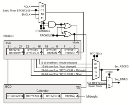
Figure 4. Real Time Clock
Real Time clocks(RTC) are used in variety of applications from watches and clocks on time stamping events and generatig events. The geenral implementation of RTC is simple. It conists of timer/counter giving 1-second interrupts and small CPU routine to count the interrupts.
The CPU can sleep or perform other functions between interrupts. The clock setup for RTC implementation uses LFXT1 oscillator in LF mode with 32768 Hz crystal. The otput of LFXT1 oscillator is selcted to source CLK . ACLK is then selected as the clock source for timer/counter that serves as the time base for RTC. The real time clock (RTC) module is used as general purpose 32 bit counter or as an RTC with calendar function selectable clock sources . It counts for seconds, minutes, hours and day of the week, day of the month and year in calendar mode.
8.1.6 ADC
An analog to digital converter is an electronic circuit converts an analog input voltage into its digital representation. The output of the ADC is an integer that is proportional to the magnitude of the sampled analog voltage and relative to an internal or external reference voltage.
Digital output = (Analog input voltage/ Reference voltage) x 2 ^(ADC bit size)
|
Figure5 . ADC 10
The analog input circuitry in microcontroller starts with analog multiplexer to support multiple of analog input and any one of the input is allowed to further block to process the analog signal. The sample and hold circuitry holds the analog voltage and holds for ADC to complete conversion. The selction of the channel in the multiplexer and controlling sample and hold circuit are done by control registers. The output of sample and hold circuit is converted into corresponding digital output and its updated to ADC result memory as well as setting the flag.
8.1.7 DAC
The DAC can be interrupt enabled via the DAC control register and the interrupt eanble register. The fals is set whenever a conversion is complete. Also the DAC output can be grouped together to ensure that the output of both DACs appears simultaneously. When the unis are grouped both DAC_12xDAT registers must be written before the outputs appear. The device does not check whether you have changed the value updating with the same information.
8.1.8 SD 16
The MSP430F42x series of ultra-low power, flash-based microcontrollers comes with three integrated 16-bit sigma-delta analog-to-digital converters (SD16). These data converters also feature an on-chip programmable gain amplifier (PGA) which allows the amplification of incoming signals up to 32 times. The bridge sensor is connected directly to the microcontroller
The MSP430 SD16 16-bit sigma-delta ADC can operate either using a built-in reference of 1.2 V, or an externally connected reference voltage as used in this application example. Here, an external resistor divider is used to provide the reference voltage.
8.1.9 LCD
MSP 430 is on-board emulation for programming and debugging the features of 14/20-pin DIP socket, on-board buttons,LEDS and Booster Pack compatible pin outs that support a wide range of plug-in modules for added functionality such as wireless displays and more.
The MSP430G2xx series are ultra low-power mixed signal microcontroller with built-in 16-bit timers, upto 24 I/O touch sense enabled pins, a versatile analog comparator, and built-in communication capability using the universal serial communication interface.
LCD Display
|
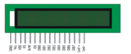
Figure6. LCD Display
A 16x2 LCD means it can display 16 characters per line and there are 2 such lines. In this LCD each character is displayed In 5x7 pixel matrix. This LCD has two registers, namely, Command and Data. The command register stores the command instructions given to the LCD. A command is an instruction given to LCD to do a predefined task like initializing it, clearing its screen, setting the cursor position, controlling display etc. The data register stores the data to be displayed on the LCD. The data is the ASCII value of the character to be displayed on the LCD.
|
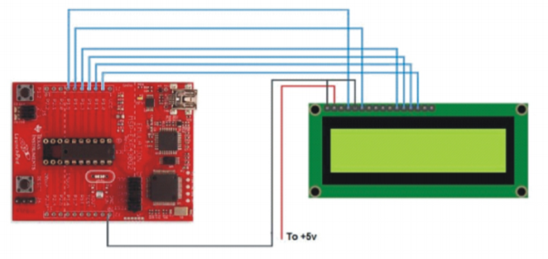
Figure 7. Interfacing
#include<msp430g2211.h>
#include”lcd16.h”
#define EN BIT4
#define RS BIT5
void Delay(volatile unsigned intx)
{
volatile unsigned int i;
for(x;x>1;x--)
{
For(i=0;i<110;i++);
}
}
void lcdcmd(unsigned char Data)
{
P1OUT & = ~RS;// because sending command
P1OUT & = ~EN;
P1OUT & = ~RS;// because sending command
P1OUT & = ~EN;
P1OUT & = 0xF0;
P1OUT | = ((Data>>4)&0x0F);
P1OUT | =EN;
Delay(2);
P1OUT & = ~EN;
P1OUT & = 0xF0;
P1OUT | = ((Data>>4)&0x0F);
P1 OUT |=EN;
Delay(2);
P1OUT&= ~EN;
}
void lcdData (unsigned char|)
{
P1OUT | = RS;// because sending data
P1OUT & = ~EN;
P1OUT & = 0x0F;
P1OUT |= (I>>4) &0x0F);
P1OUT |=EN;
Delay(2);
P1OUT & = ~EN;
P1OUT & = 0x0F;
P1OUT |= (I &0x0F);
P1OUT |=EN;
Delay(2);
P1 OUT & = ~EN;
}
void lcdinit(void)
{
P1OUT = ~RS;// because sending data
P1OUT & = ~EN;
P1OUT & = 0x3;
Delay(40)
P1OUT |=EN;
P1OUT & = ~EN;
Delay(5)
P1OUT | = EN;
P1OUT  = ~EN;
P1OUT |=EN;
Delay(2);
P1 OUT & = 0xF2;
P1OUT |=EN;
P1OUT & = ~EN;
}
lcdcmd90x28); // set data length 4 bit 2 line
Delay(250)
lcdcmd(0x0E); //set display on cursor on blink on
Delay(250)
Lcdcmd(0x01) ; // clear lcd
Delay(250)
Lcdcmd(0x06)// cursor shift direction
Delay(250)
Lcdcmd(0x80);// set ram address
Delay(250);
}
void main(void)
{
WDTCTL = WDTPW+WDTHOLD;
P1 DIR = 0xFF;
P1 OUT = 0x00;
lcdinit();
prints(“EM MEDIA”);
goto Xy(0,1) ;
while(1);
}
8.1.10 DMA
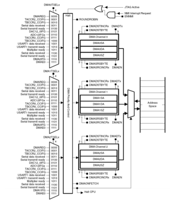
The direct memory access (DMA) controller see block diagram allows movement of data from one memory address to another, across the entire address range, without CPU intervention.
|
Figure 8. DMA configuration
DMA controller features:
Three independent transfer channels ;
Configurable DMA channel priorities
DMA transfer cycle time:
- Requires only two MCLK clock cycles per transfer.
- Each byte/word transfer requires two MCLK cycles after synchronization and one cycle of wait tome after transfer.
Byte or word and mixed byte/word transfer capability:
- Byte-to-byte;
- Word-to-word;
- Byte-to-word
- Word-to-byte (lower byte of the source word transfers).
Block sizes up to 65535 bytes or words;
Key Takeaways:
MSP430 architecture is rich in on-chip analog and digital peripherals
8.2.1 Clock System
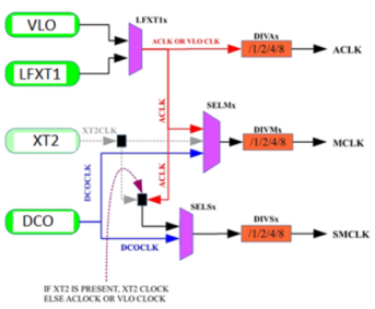
Clock sources availability depends on the version of MSP430 microcontroller.
|
Figure 9. Clock System
VLOCCLK- This is a very low power/low frequency internal oscillator that can produce a frequency of 10KHz.
LFXT1CLK- (Low Frequency Crystal) – It is a crystal powered low/high frequency oscillator. It can work with either a 32Khz crystals that operate in the MHz range or external clock sources (400KHz to 16MHz range)
XT2CLK(High frequency crystal)- This is a high frequency oscillator that can be used with standard crystals resonator or external clock sources in the 400Khz to 16 MHz range.
DCOCLK- Integrated Digitally Controlled Oscillator do not use any external crystals. The DCO can generate a wide variety of frequencies ranging from few 100-kilo hertz to 10’s of MHz. It is default clock of the MSP430 after reset. The DCO clock frequency is temperature dependent.
MSP430 produces 3 different clock signals using a combination of the oscillator sources. These clock signals can be used to various peripherals like CPU, Timers, ADC etc depending upon the requirements.
MCLK- Known as main clock. It is fast high frequency clock usually used by CPU or other fast components like ADC10,ADC12, Watch Dog timer. MCLK can be sources either from LFT1CLK,DCO,VLO or XT2 oscillator. Clock signal can be divided by 1/2/4/8 using internal divider.
SMCLK- Known as Sub Main Clock. It can be sources either from LFT1CLK,DCO,VLO or XT2 oscillator. Clock signal can be divided by 1/2/4/8 using internal divider.
ACLK- known as Auxillary clock is slow,low frequency clock . It can only be sourced from LFT1CLK or VLO. Clock signal can be divided by 1/2/4/8 using internal divider. ALCK is active in all Low power modes except LPM4.
8.2.2 Low Power Modes
MSP430 works on two types of mode:
- Active Mode
- Low Power Modes(Standby mode)
MSP430 is designed for ultralow power applications. It offers the lowest power consumtion and perfect mix of integrated peripherals for a variety of battery operated applications.
It has Low power modes LPM 0,1,2,3,4, and 3.5 and 4.5. AM is the normal running mode and all LPM for low power consideration modes. The low power operating modes consider the needs of ultralow-power consumtion, speed, data throughput and minimization of individual peripheral current consumption.
LPM0- Both CPU and MCLK are disabled. SMCLK and ACLK remain active. Peripherals which use SMCLK and ACLK also remain active.
LPM1- Both CPU and MCLK are diabled . DCO is disabled . SMCLK is not available if it is sourced from DCO , ACLK remains active.
LPM2- CPU,MCLK,SMCLK and DCO are disabled,ACLK remain active.
LPM3 – CPU,MCLK,SMCLK,DCO are disabled, ACLK remain active.
LPM4- All the clocks including ACLK are disabled in this mode. The controller can only be wakened from this mode by an external interrupt. This mode consumes the least power compared to all other modes.
8.2.3 Clock Request Feature
The Launchpad typically uses a MSP430G2553 device that contains a Basic Clock Module+. XT1 supports both low frequency and high frequency crystals, and it integrates both DCOCLK and VLOCLK.
After power-up, MCLK and SMCLK are sourced from DCOCLK at about 1.1MHz. ACLK is sourced from LFXT1CLK in LF mode. The Launchpad comes with an option 32kHz crystal in the box that needs to be installed by the user.
|
Fig 10.Pin 18 and Pin 19 are XIN and XOUT and allow an external crystal to be connected, either 32kHz or a fast crystal.
The following code makes P2.6 and P2.7 set for accepting a crystal at the input:
MSP430 Using External 32kHz crystal
#include <msp430.h>
void main()
{
WDTCTL = WDTPW + WDTHOLD; // Stop watchdog timer
P2SEL |= (BIT6 | BIT7); // Set P2.6 and P2.6 SEL for XIN, XOUT
P2SEL2 &= ~(BIT6|BIT7); // Set P2.6 and P2.7 SEL2 for XIN, XOUT
/* Select 32kHz Crystal for ACLK */
BCSCTL1 &= (~XTS); // ACLK = LFXT1CLK
BCSCTL3 &= ~(BIT4|BIT5); // 32768Hz crystal on LFXT1
/* Output buffered ACLK on P1.0 */
P1SEL |= BIT0;
P1SEL2 &= ~(BIT0);
P1DIR |= BIT0;
}
8.2.4 Low power programming and Interrupt.
To enable low power the MSP430 supports several modes, each shutting off the MSP430 more and more:
- Active Mode (AM) – Not a low power mode but rather the mode in which everything is turned on, except perhaps for some peripherals
- LPM0 – CPU and MCLK are shutoff. SMCLK and ACLK remain active.
- LPM1 – CPU and MCLK are off, as in LPM1, but DCO and DC generator are disabled if the DCO is not used for SMCLK. ACLK is active.
- LPM2 – CPU, MCLK, SMCLK and DCO are disabled, while DC generator is still enabled. ACLK is active.
- LPM3 – CPU, MCLK, SMCLK, DCO and DC generator are disabled. ACLK is active.
- LPM4 – CPU and all clocks disabled
These LPM modes refer to the individual bits in the Status Register. By setting and clearing the bits in the SR, one can turn off CPU and clocks resulting in certain Low Power Modes.
To see the power consumption
|
Figure11. Power Consumption
At 1MHz, we go from 300uA down to less than 1uA by switching to LPM3. This is what makes the MSP430 such a good microcontroller for low power applications. It can survive for years on batteries.
Key Takeaway:
Low power operation is a key feature of the MSP430. Its design gives very low leakage, and it operates from a single supply rail.
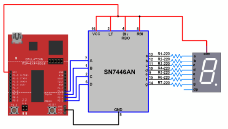
8.3.1 Seven Segment LED modules interfacing
7-segment displays are made up of 8 LED segments. They are used to display Numbers (0-9) and certain Alphabets (like c, A, H, P, etc.).
- 7 of these LED segments are in the shape of a line, whereas 1 segment is circular.
- Each of the 8 elements has a pin associated with it which can be driven HIGH or LOW.
- To display a number or alphabet, we need to turn on specific LED segments of the display.
|
Figure . 12 segment display interfacing
int bcd_pins[4]; /* array for A-D pins of driver IC */
void bcd_control_pins(int a, int b, int c, int d) /* Assigns A-D pins of deiver IC to TI Launchpad */
{
bcd_pins[0] = a;
bcd_pins[1] = b;
bcd_pins[2] = c;
bcd_pins[3] = d;
}
void display_number(int num) /* Function for displaying number (0-9) */
{
switch(num)
{
case 0:
digitalWrite(bcd_pins[0], LOW); /* Drive bcd_pin[0] to LOW */
digitalWrite(bcd_pins[1], LOW); /* Driving LOW turns on LED segment for common anode display */
digitalWrite(bcd_pins[2], LOW);
digitalWrite(bcd_pins[3], LOW);
break;
case 1:
digitalWrite(bcd_pins[0], HIGH);
digitalWrite(bcd_pins[1], LOW);
digitalWrite(bcd_pins[2], LOW);
digitalWrite(bcd_pins[3], LOW);
break;
case 2:
digitalWrite(bcd_pins[0], LOW);
digitalWrite(bcd_pins[1], HIGH);
digitalWrite(bcd_pins[2], LOW);
digitalWrite(bcd_pins[3], LOW);
break;
case 3:
digitalWrite(bcd_pins[0], HIGH); /* Drive bcd_pin[3] to HIGH */
digitalWrite(bcd_pins[1], HIGH); /* Driving HIGH turns on LED segment for common anode display */
digitalWrite(bcd_pins[2], LOW);
digitalWrite(bcd_pins[3], LOW);
break;
case 4:
digitalWrite(bcd_pins[0], LOW);
digitalWrite(bcd_pins[1], LOW);
digitalWrite(bcd_pins[2], HIGH);
digitalWrite(bcd_pins[3], LOW);
break;
case 5:
digitalWrite(bcd_pins[0], HIGH);
digitalWrite(bcd_pins[1], LOW);
digitalWrite(bcd_pins[2], HIGH);
digitalWrite(bcd_pins[3], LOW);
break;
case 6:
digitalWrite(bcd_pins[0], LOW);
digitalWrite(bcd_pins[1], HIGH);
digitalWrite(bcd_pins[2], HIGH);
digitalWrite(bcd_pins[3], LOW);
break;
case 7:
digitalWrite(bcd_pins[0], HIGH);
digitalWrite(bcd_pins[1], HIGH);
digitalWrite(bcd_pins[2], HIGH);
digitalWrite(bcd_pins[3], LOW);
break;
case 8:
digitalWrite(bcd_pins[0], LOW);
digitalWrite(bcd_pins[1], LOW);
digitalWrite(bcd_pins[2], LOW);
digitalWrite(bcd_pins[3], HIGH);
break;
case 9:
digitalWrite(bcd_pins[0], HIGH);
digitalWrite(bcd_pins[1], LOW);
digitalWrite(bcd_pins[2], LOW);
digitalWrite(bcd_pins[3], HIGH);
break;
default:
digitalWrite(bcd_pins[0], LOW);
digitalWrite(bcd_pins[1], LOW);
digitalWrite(bcd_pins[2], LOW);
digitalWrite(bcd_pins[3], LOW);
break;
}
}
void setup() {
pinMode(11, OUTPUT);
pinMode(12, OUTPUT);
pinMode(13, OUTPUT);
pinMode(14, OUTPUT);
bcd_control_pins(14,13,12,11); /* A-D of driver IC to TI Launchpad */
}
void loop() {
int i;
for(i = 9; i>=0; i--)
{
display_number(i);
delay(1000);
}
for(i = 0; i<=9; i++)
{
display_number(i);
delay(1000);
}
}
Key Takeaways:
Indicators and displays are important in projects as it allows us to know whether the data that is the input has been processed correctly or not
8.4.1 Data Acqistion system
The most basic form of data acquisition is digital input and digital output. To setup a pin as a digital input or output, one must configure that pin to accept or produce a voltage. In the following table, Figure 1, each of the important registers are listed alongside their functions. In the code that follows, it should be noted that BIT5 denotes a ‘1’ on the registers 5th bit, and ~BIT5 denotes a ‘0’ on the registers 5th bit
|
In the following example, pin P1.5 is configured as an input. A loop is constantly checking the pin for an input voltage.
For an input to read ‘1’, the voltage must be between 2 and 5 Volts.
Between 0 and 1.3 Volts the input will be read as ‘0’.
Between 1.3 and 2 Volts, the digital value of the bit will not change.
void main(void)
{
P1SEL = ~BIT5; //P1.5 is I/O
P1DIR = ~BIT5; //
P1.5 is input
//main loop
while (1)
{
if (P1IN & BIT5 == BIT5)
{
//input detected, execute logic
}
else
{
}//input not detected, execute logic
} //end while
} //end main
8.4.2 Wired Sensor network
Patient monitoring system using MSP430 microcontroller .MSP430 micro controller is a low power microcontroller. MSP430 microcontroller is 16 bit. And it is a RISC based, and also is a mixed signal processor. MSP430 microcontroller mainly has three types low current modes. SMCLK ,ACLK ,MCLK these are three low current modes. The ethernet controller allows many computers from single station to one another through network. This networking is done with the help of Ethernet protocols and Ethernet hardware. The main benefit of Ethernet is it can sense collision on the network. Processing ability of MSP430 micro controller is very strong, simulation technology performance is very high these are the advantages of MSP430 microcontrollers. Features of ethernet controller are-to avoid collision and It support both full duplex and half duplex modes.
8.4.3 Wireless sensor network with Chipcon RF interfaces
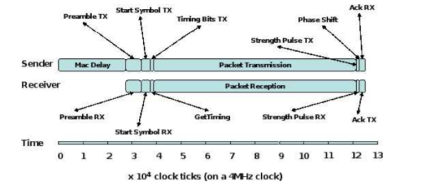
The Tmote Sky utilizes an early IEEE 802.15.4 protocol for mesh networking using a Chipcon SmartRF CC2420 ZigBee-ready wireless transceiver. This transceiver is a low-cost solution for providing robust wireless communication in the unlicensed ISM band. The transceiver provides many desirable features, including a physical protocol, a MAC protocol, and AES encryption. These features are used by the Tmote Sky for its TinyOS mesh networking implementation . The Chipcon CC2420 transceiver interacts directly with TinyOS, allowing the Tmote platform to abstract the networking algorithms from the programmer. Simply specifying a destination node identifier in the NesC program allows TinyOS to transparently rout packets to the correct node, regardless of its location on the mesh network. Between the TinyOS code and the Chipcon transceiver, 11 the packets sent and received by the Tmote units appear similar to packets from any network. This includes the basic format of MAC, preamble, and data followed by an acknowledgement packet. This basic behaviour is outlined in a timing diagram depicted in Figure . This method of transmission is typical of most networks, wireless or otherwise, and speaks to the reliability of the Tmote Sky’s wireless networking capabilities.
|
Figure 13: Timing diagram of network transmission and reception
Key Takeaways:
This microcontroller uses ultra-low power and consists of analog and digital devices for sensing and measurement applications
References:


