Unit 1
SEMICONDUCTOR DIODES AND APPLICATIONS
V Barrier
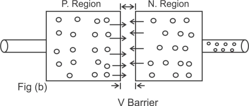
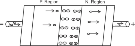
- A Forward biased showing the flow of majority carriers and the voltage due to the barrier potential across the depletion region-
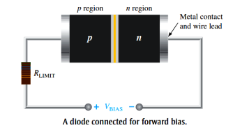
- To bias a diode apply d,c vtg across it .
- Forward bias is the condition that allows current through the PN junction.
- Negative side of VBIAS is connected to the N -region of the diode and the positive side is connected to the P- region.
- A selected requirement is that the bias voltage VBIAS must be greater than the barrier potential.
- Because of like charges repel ,the negative side of the bias voltage source pushes the free electrons , which are the majority carriers in the N-region towards the PN junction .the flow of free is called Electron Current.
- The –Ve side of the source also provide a continues flow of electrons through the external connection (conductor).
- Into the N-region as show in fig-B
- The bias voltage source imparts sufficient energy to the free electrons for them to overcome the barrier potential of the depletion region and move on through into the 'p' region once in the P-region .these conduction electrons have lost enough energy to immediately combine with holes in the valence band.
- Now the e- are in the valance band in the P-region simply because they have lost too much energy overcoming the barrier potential to remain in the conduction band. Since unlike charge attract, the positive side of the bias voltage source attracts the valence electrons toward the left end of the region.
- The hole in the P-region provide the medium or "Pathway" for these valence electrons to move through the P-region.
- The holes which are the majority carriers in the P-region , effectively (not actually ) move to the right toward the junction as shown in fig-B.
- The defective flow of holes is called the hole current.
- As from Fig-B hole current as the flow of valence electrons through the P-region with the holes providing the only means for these electrons to flow.
- As the electrons flow out of the P-region through the external connection and to the positive side of the bias in the P-region at the same time these electrons become conduction electrons in the mater conductor .
- To these is a continues availability of holes effectively moving towards the PN junction stream of electrons as they come across the junction in to the P-region.
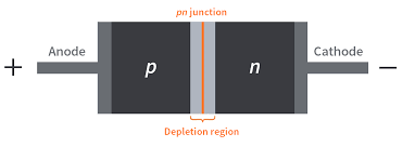
The effect of forward bias on the depletion region:-


+ -


 -
-
Depletion Region
- Forward bias narrows the depletion region & produce a vtg drop across pn junction equal to the barrier potential.
- As more electrons flow into the depletion region , the number of positive ions is reduce . As more notes effectively flow into the depletion region on the other side of the pn junction ,the number of -ve ions is reduce this reduction in positive & -ve ions during forward bias causes the depletion region to narrow.
The Effect of the Barrier Potential during forward bias:-
- The electronic field between the positive and negative ions in the depletion region on either side of the junction creates an energy bill, that prevent free R form diffusing across the junction at equilibrium this is known as the barrier potential
- When forward bias is applied the free electrons are provided with enough energy from the bias voltage source to over come the barrier potential and effectively climb the energy bill and cross the depletion region.
- The energy that the electronics repair in order to pass through the depletion region is equal to the barrier potential.
- Electron gives up an amount of energy equivalent to the barrier potential when they cross the depletion region.
- This energy loss results in a vtg drop across the pn junction equals to the barrier potential (0.7v)
- An additional small vtg drop across the P & N regions due to the internal resistance of the material.
- For doped Semiconductor material ,this resistance called the dynamic resistance is very small and can usually be neglected.
REVERSE BIAS:-
Reverse bias is the condition the essentially prevents current through the diode.


P-region N- region


- +
V BIAS
A Diode connected for Reverse Biased-
- Because unlike charges attract the positive side of the bia voltage source pulls the free election , which are the majority carriers in the N-region away from the PN junction.
- AS the election flow towards the positive side of the voltage source additional positive ions are created
- This results in a widening of the depletion region and a depletion of majority carriers.


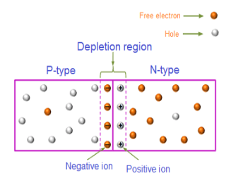
- The diode during the short transition time immediately after reverse bias vtg is applied-
- In the P-region electrons from the negative side of the vtg source enter as valence electron and move from hole to hole toward the depletion region where the creators additional -ve ions.
- This results in a widening of the depletion region and a depletion of majority carriers
- As the depletion region widens the availability of majority carriers decreases
- As more of the N & P regions become depleted of majority carriers ,the electric field between the positive and -ve ions increase in strength the depletion region equals the bios vtg .this point the transition current essentially ceases except for a small reverse current that can usually be neglected.
Reverse Current
- Extremely small current that exist in reverse bias after the transition current dies act is caused by the minority carrier in the N& P region that are produced by the manly generated e hole pairs.
- The conduction band in the P-region is at a higher energy level then the conduction band in the N-region . Therefore the minority easily pass through the depletion region because they required no additional energy.
The Extremely small reverse current in a reverse biased diode is due to the minority carriers from thermally generated
e=hole pairs
To define the dc diode model, the characteristics of an ideal diode and modifications are required for practical considerations.
¾ Ideal diode: VON = 0, Rr = ∞ and Rf = 0.
The ideal diode is a short in the forward bias region and an open in the reverse bias region. ¾ Practical diode (silicon): VON = 0.7V, Rr < ∞ (typically several MΩ), Rf ≈ rd (typically < 50 Ω).
The general representation for a practical diode under dc operating conditions is shown below. The diode is a two-terminal device, which simply means that it connects to other circuit elements at connection points labeled a and b in the circuit below with the voltage Vab applied across the diode.
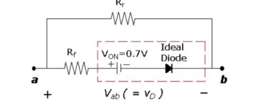
This model may be simplified if we can define the operating region as forward or reverse bias.
For the forward bias region (vD ≥ 0.7 V for silicon), the ideal diode is a short and the terminal characteristics of the model above reduce to the parallel combination of Rr and Rf.
Since Rr >> Rf, Rr ||Rf ≈ Rf.
Likewise, when the voltage applied to the diode is less than VON (vD < 0.7 V for silicon), the ideal diode is an open and the resistance between terminals a and b is Rr.

Forward biased dc model Reverse biased dc model
AC Diode Model:
The charge separation comes about in the diode due to the depletion region, which is in turn dependent on the applied bias. For the reverse bias case, this introduces a junction capacitance (Cj) in parallel with the reverse bias resistance (Rr) as shown below and in Figure.
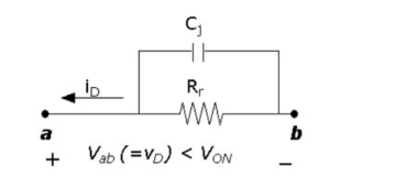
Reverse biased AC model
The frequency of operation introduces an additional consideration for forward bias operation. The current flows in different directions under ac operation. Since current flow is moving charge, there are charges moving in the semiconductor material. Charges cannot move instantaneously, so there
Is a “charge storage” effect that leads to a diffusion capacitance (CD). The forward bias resistance is also a function of frequency, so the dynamic resistance, rd, of Equation which replaces the constant Rf term.
Hence the ac diode model under forward bias conditions is represented below
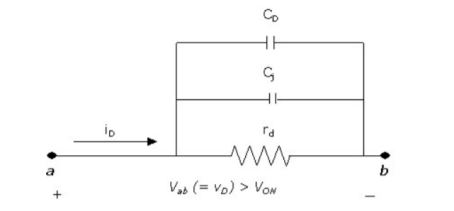
Forward biased AC model
- Zenor diode is a special type of p-n junction semiconductor diode in this diode the reverse breakdown voltage is adjusted precisely between 3v to 200v.
- Its applications are based on this principle hence zenor diode is called as a breakdown diode.
- The doping level of the imparity added to manufacture the zener diode is controlled in order to adjust the precise value of breakdown voltage.
PRINCIPLE OF OPERATION:- A zener diode can be forward biased or reverses biased. Its operation in the forward biased mode is same as that of a p-n junction diode but its operation in the reverse biased mode is sustainably deferent.

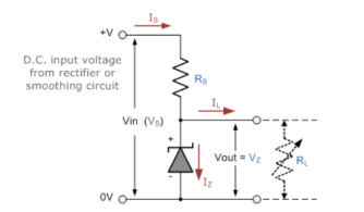
- The resistor, RS is connected in series with the Zener diode to limit the current flow through the diode with the voltage source, VS being connected across the combination. The stabilised output voltage Vout is taken from across the Zener diode.
- The Zener diode is connected with its cathode terminal connected to the positive rail of the DC supply so it is reverse biased and will be operating in its breakdown condition. Resistor RS is selected so to limit the maximum current flowing in the circuit.
- The load is connected in parallel with the Zener diode, so the voltage across RL is always the same as the Zener voltage, ( VR = VZ ).
- There is a minimum Zener current for which the stabilisation of the voltage is effective, and the Zener current must stay within the value operating under load within its breakdown region at all times.
- The upper limit of current is of course dependent upon the power rating of the device. The supply voltage VS must be greater than VZ.
- A Zener diode is always operated in its reverse biased condition. As such a simple voltage regulator circuit can be designed using a Zener diode to maintain a constant DC output voltage across the load despite variations in the input voltage or changes in the load current.
- The Zener voltage regulator consists of a current limiting resistor RS connected in series with the input voltage VS with the Zener diode connected in parallel with the load RL in this reverse biased condition.
- The stabilised output voltage is always selected to be the same as the breakdown voltage VZ of the diode.
A 5.0V stabilised power supply is required to be produced from a 12V DC power supply input source. The maximum power rating PZ of the zener diode is 2W. Using the zener regulator circuit above calculate:
a). The maximum current flowing through the zener diode.
Maximum current = Watts/ Voltage = 2w/ 5V = 400mA
b). The minimum value of the series resistor, RS
Rs = Vs – Vz/ Iz = 2 – 5 / 400mA = 17.5 Ω
c). The load current IL if a load resistor of 1kΩ is connected across the zener diode.
IL = Vz / RL = 5v/ 1000Ω = 5mA
d). The zener current IZ at full load.
IZ = Is – IL = 400 mA – 5mA = 395mA
1)Due to the unidirectional current flow through the transformer there is a possibility of core saturation to avoid this transformer size must be increased.
2)Ripple factor is high.
3)Low rectification effecting.
4)Law TUF.
5)Law D.C O/P VTG & current.
6)Large filter component are required.
ADVANTAGES:-
1)Simple Construction.
2) Component required less.
3)Small size.
APPLICATION:-
Walkman, law cost power supply.
TRANSFORMER UTILISATION FACTOR(TUF) :-It indicates how well the ilp transformer is being utilized
TUF= DC O/P Power / AC power rating of the transformer

1)A center tapped rectifier is a type of full wave rectifier that uses two diode connected to the secondary of a center tapped transformer.
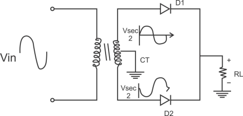
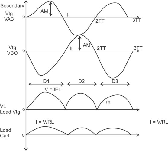
Center tapped full wave rectifier operation:-
I) During positive half cycle of i/p ac supply.
Diagram

D1.Is in forward biased & D2 is in reverse biased.
II)During -ve half cycle.

D1 Reverse biased
D2 Forward biased
ADVANTAGES
1) law ripple factor as Compared to HKR.
2)Better rectification efficiency.
3) Better TUF.
4)Higher value of average load vtg & avg load crt.
5)No possibility of transformer core saturation.
DISADVANTAGES
PIV of diode is 2vm , more size costly.
APPLICATION
I) Battery charges.
2)power supply at laboratory, high current, electronic ckt.
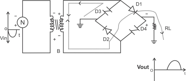
The bridge rectifier uses four diode connected, when the i/p cycle is positive diode D1 & D2 are forward biased and conduct current in the direction shown a vtg is developed across RL which looks the positive half of the i/p cycle during this diodes D3 and D4 are reverse biased.
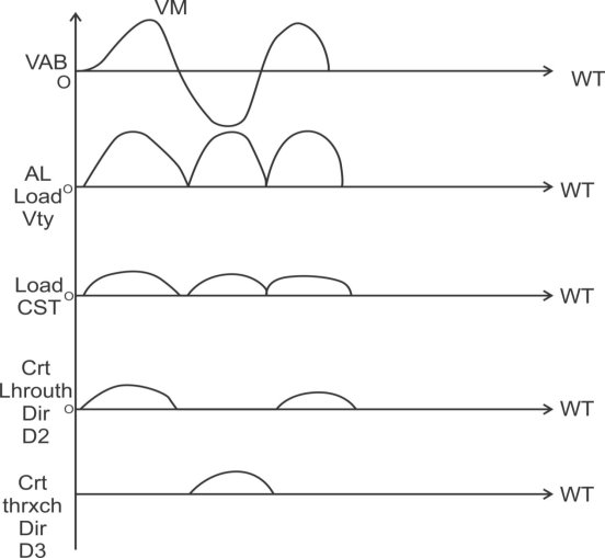
When the ilp cycle is -ve diode D3& D4 are forward biased & conduct current in the same direction through R1 as during in the positive half cycle during the -ve half cycle D1& D2 are reverse biased. a full wave rectified O/P VTG appears across RL as a result of this action.
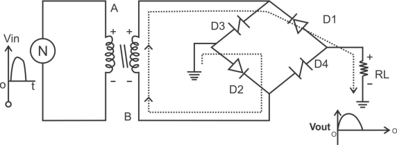
- during positive half cycle of ilp D1 & D2 are forward biased conduct current D3 & D4 are reverse biased:-
- during -ve half cycle of the ilp D3 &D4 are forward biased & conduct current D1 & D2 are reverse biased-
NOTE - Practically vp(out)= vp sec-1.4v 1000 diode knee vtg.
Advantages :-
1) It require a small size transformer center tap transformer is not required .this makes the bridge rectifier cost effective.
2) This ckt is most suitable for the high vtg application . This is because the max -ve that appears across each diode is -vm therefore the diode with PIV rating of -vm volts are required to be selected (PIV in fall wave rectifier is 2vm
3) Core saturation does not take place.
4) High TUF, high avg, vtg
Disadvantages :-
1)Number of diode used is four instead two for FWR
2)As two diodes conduct simultaneously , the vtg drop increase and the o/p vtg reduces.
Applications :-
Laboratory , high current, battery , electronic , ckt power supply.
- A typical capacitor filter circuit diagram is shown below. The designing of this circuit can be done with a capacitor as well as load resistor (RL).
- The rectifier’s exciting voltage is given across the terminals of a capacitor. Whenever the voltage of the rectifier enhances then the capacitor will be charged as well as supplies the current to the load.
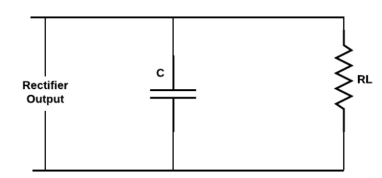
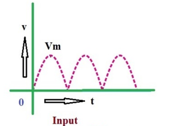
- At the last part of the quarter phase, the capacitor will be charged to the highest rectifier voltage value that is denoted with Vm, and then the voltage of the rectifier starts to reduce.
- As this happens, the capacitor starts discharging through the voltage across it and load. The voltage across the load will reduce little only because the next peak voltage occurs instantaneously to charge the capacitor.
- This procedure will repeat many times and the output waveform will be seen that very slight ripple is missing in the output.
- The output voltage is superior because it remains significantly close to the highest value of the output voltage of the rectifier.
A capacitor gives an infinite reactance to DC. For, DC, f=0
Xc = 1/ 2пfc = 1/2п x 0 x C = infinite
Therefore, a capacitor does not permit DC to flow through it.
The photodiode is a p-n junction semiconductor diode which is always operated in the reverse biased condition.
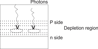
The light is always focused through a glass lens on the junction of the photodiode As the photodiode is reverse biased the depletion region is quite wide, penetrated on both side of the junction.
The photons incident on the depletion region will impact their energy to the Ions present in depletion region and generates e hole pairs.
The photons incident on the depletion region so the number of electron hole pairs will be generated depends on the intensity of light [number of photons] These and holes will be attracted towards the +ve& -ve terminals respectively of the photo current ,
With increase in the light intensity more number of e hole pairs are generated and the photo current increases thus the photocurrent is proportional to the light intensity.
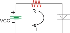
An LED emits light when electrical energy is applied to it. For proper operation it is necessary to forward bias the LED.
Construction of LED :-
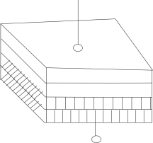
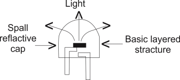
To make emission of light in one direction cup type construction is used for LED.
PRINCIPLE LED OPERATION
When the led is forward is forward biased the electrons in the n-region will cross the junction and recombine with the holes in the p- type material.
These free e- reside in the conduction band & hence at a higher energy level than the holes in the valence band
When recombination takes place this e- return peak to the valence band which is at a lower energy level than the conduction band.
While returning back the recombining e-give away the excess energy in the form of light . This process is called as electroluminescence. In this way an LED emits light.
Color of the Emitted Light
Material Use Color of Emitted Light
i)Gallium Arsenide (GOAS) In fared (IR)
Ii) GaASP(gallium arsenide Red or Yellow
Phosphide)
Iii) Gallium phosphide (GAP) Red or Green
Application
Used in 7 Segment Display
An optocoupler or opto-isolator consists of a light emitter, the LED and a light sensitive receiver which can be a single photo-diode, photo-transistor, photo-resistor, photo-SCR, or a photo-TRIAC with the basic operation of an optocoupler.
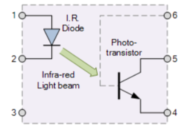
Assume a photo-transistor device as shown. Current from the source signal passes through the input LED which emits an infra-red light whose intensity is proportional to the electrical signal.
This emitted light falls upon the base of the phototransistor, causing it to switch-ON and conduct in a similar way to a normal bipolar transistor.
The base connection of the photo-transistor can be left open (unconnected) for maximum sensitivity to the LEDs infra-red light energy or connected to ground via a suitable external high value resistor to control the switching sensitivity making it more stable and resistant to false triggering by external electrical noise or voltage transients.
When the current flowing through the LED is interrupted, the infra-red emitted light is cut-off, causing the phototransistor to cease conducting.
The phototransistor can be used to switch current in the output circuit. The spectral response of the LED and the photo-sensitive device are closely matched being separated by a transparent medium such as glass, plastic, or air.
Since there is no direct electrical connection between the input and output of an optocoupler, electrical isolation up to 10kV is achieved.
The voltage regulator IC 7805 is actually a member of the 78xx series of voltage regulator ICs. It is a fixed linear voltage regulator.
The xx present in 78xx represents the value of the fixed output voltage that the particular IC provides.
For 7805 IC, it is +5V DC regulated power supply. This regulator IC also adds a provision for a heat sink.
The input voltage to this voltage regulator can be up to 35V, and this IC can give a constant 5V for any value of input less than or equal to 35V which is the threshold limit.
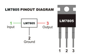
PIN 1-INPUT
The function of this pin is to give the input voltage. It should be in the range of 7V to 35V. We apply an unregulated voltage to this pin for regulation. For 7.2V input, the PIN achieves its maximum efficiency.
PIN 2-GROUND
We connect the ground to this pin. For output and input, this pin is equally neutral (0V).
PIN 3-OUTPUT
This pin is used to take the regulated output.
It will be 5V(4.8 V – 5.2 V)
In IC 7805 voltage regulator, lots of energy is exhausted in the form of heat. The difference in the value of input voltage and output voltage comes as heat.
So, if the difference between input voltage and the output voltage is high, there will be more heat generation.
Without a heat sink, this too much heat will cause malfunction.
The bare minimum tolerable difference between the input and output voltage to keep the output voltage at the proper level as dropout voltage.
It is better to keep the input voltage 2 to 3V greater than the output voltage, or a suitable heat sink should be placed to dissipate excess heat.
To calculate the heat sink size properly. The following formula is used
Heat generated = (input voltage -5) x output current.
The relation of generated heat and the input voltage value in this regulator with the following two examples.
Assume a system with input voltage 16V and required output current be 0.5A.
So, heat generated (16-5 ) x 0.5 = 5.5 W
Thus, 5.5W heat energy is wasted, and the actual energy used V x I = 5 x 0.5 = 2.75 W
That is almost double energy is wasted as heat.
Next, we can consider the case when input is lower, say 9V.
In this case, heat generated
(9-5) x 0.5 = 2 W.
Internal Block Diagram of 7805 IC
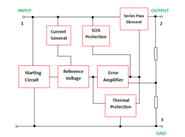
The block diagram comprises of an error amplifier, series pass element, current generator, reference voltage, current generator, starting circuit, SOA protection and thermal protection.
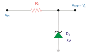
Here the operating amplifier performs as an error amplifier. The Zener diode is used for giving the reference voltage.
It is shown below.
Transistor is the series pass element here. It is used for dissipating additional energy in the form of heat.
- It controls the output voltage by controlling the current among the input and output. SOA is the Safe Operating Area.
- It is in fact the conditions of voltage and current in which the equipment is expected to work without any self-damage.
- Here for the SOA protection, bipolar transistor is implemented with a series resistor and an auxiliary transistor.
- Heat sink is implemented for thermal protection when there is high supply voltage.
The voltage regulator 7805 and the other components are arranged in the circuit as shown in figure.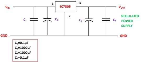
C1– It is the bypass capacitor, used to bypass very small extent spikes to the earth.
C2 and C3– They are the filter capacitors. C2 is used to make the slow changes in the input voltage given to the circuit to the steady form. C3 is used to make the slow changes in the output voltage from the regulator in the circuit to the steady form. When the value of these capacitors increases, stabilization is enlarged. But these capacitors single-handedly are unable to filter the very minute changes in the input and output voltages.
C4– like C1, it is also a bypass capacitor, used to bypass very small extent spikes to the ground or earth. This is done without influencing other components.
Applications of Voltage Regulator 7805 IC
- Current regulator
- Regulated dual supply
- Building circuits for Phone charger, UPS power supply circuits, portable CD player etc
- Fixed output regulator
- Adjustable output regulator etc.
Want More Electrical Knowledge?
Enter your email below to receive FREE informative articles on Electrical &
References:Scroll back to top
ELECTRONIC DEVICES AND CIRCUITS by VENKATA RAO, McGraw Hill
Getting started in Electronics by Forrest.M.Mims
All New Electronics – Self Teaching Guide by Harry Kybett & Earl Boysen
Practical Electronics for Inventors by Paul Scherz