Unit 2
FET AND SCR
- JFET is a current controlled device which allows current to pass from source to drain.
- The controlling voltage is applied between gate and source.
- The channel is an N-type or P-type semiconductor material.
All field-effect transistors are unipolar rather than bipolar devices. That is, the main current through them is comprised either of electrons through an N-type semiconductor or holes through a P-type semiconductor.
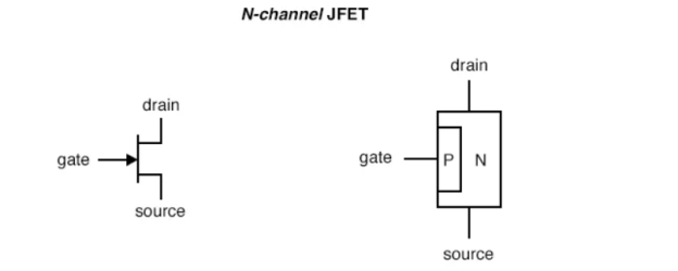
In JFET, the controlled current passes from source to drain, or from drain to source. The controlling voltage is applied between the gate and source.
The current does not have to cross through a PN junction on its way between source and drain: the path (called a channel) is an uninterrupted block of semiconductor material.
P-channel JFET
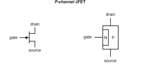
N-channel JFET are more commonly used than p-channel.
When no voltage is applied between the gate and source the channel is wide-open path for current to flow.
If voltage is applied between the gate and source the PN-junction is reverse biased and there is a flow between the source and the drain which becomes regulated.
Maximum gate to source voltage pinches off all current through source and drain forcing JFET into cut-off mode.
This behavior is due to the depletion region of the PN junction expanding under the influence of a reverse-bias voltage, eventually occupying the entire width of the channel if the voltage is great enough.
When the gate-source PN junction is reverse biased there is zero current through the gate connection. Hence JFET is voltage- controlled device.
If the gate-source PN junction is forward-biased with small voltage the JFET channel will open allowing more current to flow through.
JFET is a three terminal semiconductor device in which current conduction is by one type of carrier that is electrons or holes.
The current conduction is controlled by means of an electric field between the gate and the conducting channel of the device.
The JFET has high input impedance and low noise level.
Construction Details:
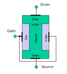
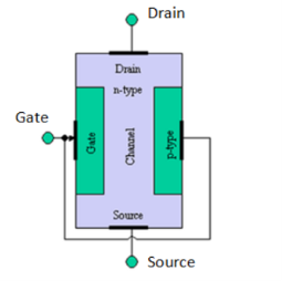
A JFET consists of a p-type or n-type silicon bar containing two p-n junctions at the sides as shown in figure.
p-type n-type
The bar forms the conducting channel for the charge carriers.
If the bar is of p-type, it is called p-channel JFET as shown in fig.a and if the bar is of n-type, it is called n-channel JFET as shown in fig.b.
The two p-n junctions forming diodes are connected internally and a common terminal called gate is taken out.
Other terminals are source and drain
Thus, a JFET has three terminals such as gate (G), source (S) and drain (D).
Fig. (i) shows the n-channel JFET polarities and fig. (ii) shows the p-channel JFET polarities.
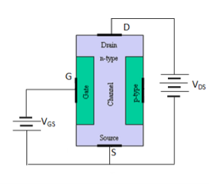
Fig. (i)
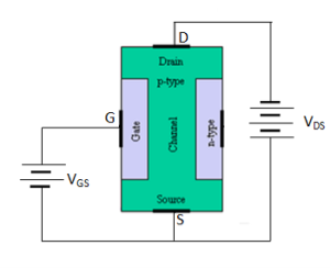
Fig. (ii)
In each case, the voltage between the gate and source is such that the gate is reverse biased.
The source and the drain terminals are interchangeable.
The following points may be noted:
- The input circuit gate to source of a JFET is reverse biased. This means that the device has high input impedance.
- The drain is so biased with respect to source that drain current ID flows from the source to drain.
- In all JFETs, source current IS is equal to the drain current that is IS = ID.
Principle and Working of JFET
The figure shows the circuit of n-channel JFET with normal polarities.
The two p-n junctions at the sides form two depletion layers.
The current conduction by charge carriers that is the electrons is through the channel between the two depletion layers and out of the drain.
The width and hence resistance of this channel can be controlled by changing the input voltage VGS.
The greater the reverse voltage VGS, the wider will be the depletion layer and narrower will be the conducting channel.
The narrower channel means greater resistance and hence source to drain current decreases.
Reverse will happen when VGS decreases.
Thus, JFET operates on the principle that width and hence resistance of the conducting channel can be varied by changing the reverse voltage VGS.
In other word, the magnitude of drain current ID can be changed by altering VGS.
The working of JFET can be explained as follows:
Case-i:
When a voltage VDS is applied between drain and source terminals and voltage on the gate is zero as shown in fig.(i), the two p-n junctions at the sides of the bar establish depletion layers.
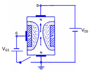
Fig. (i)
The electrons will flow from source to drain through a channel between the depletion layers.
The size of the depletion layers determines the width of the channel and hence current conduction through the bar.
Case-ii:
When a reverse voltage VGS is applied between gate and source terminals, as shown in fig.(ii), the width of depletion layer is increased.
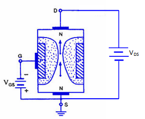
Fig. (ii)
This reduces the width of conducting channel, thereby increasing the resistance of n-type bar.
Consequently, the current from source to drain is decreased.
On the other hand, when the reverse bias on the gate is decreased, the width of the depletion layer also decreases.
This increases the width of the conducting channel and hence source to drain current.
A p-channel JFET operates in the same manner as an n-channel JFET except that channel current carriers will be the holes instead of electrons and polarities of VGS and VDS are reversed.
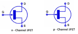
Schematic Symbol of JFET
Fig.shows the schematic symbol of JFET.
Advantages of JFET
A JFET is a voltage controlled, constant current device in which variation in input voltage control the output current.
Some of the advantages of JFET are:
- It has a very high input impedance. This permits high degree of isolation between the input and output circuits.
- The operation of a JFET depends upon the bulk material current carriers that do not cross junctions. Therefore, the inherent noise of tubes and those of transistors are not present in a JFET.
- A JFET has a negative temperature co-efficient of resistance. This avoids the risk of thermal runaway.
- A JFET has a very high power gain. This eliminates the necessity of using driver stages.
- A JFET has a smaller size, longer life and high efficiency
Drain Characteristics
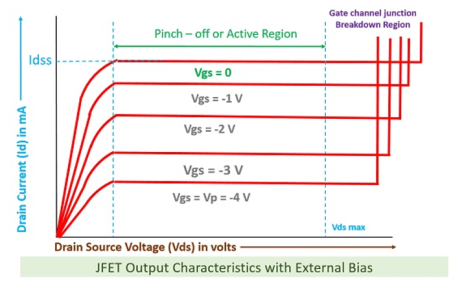
In the absence of external bias: When there is no voltage between gate and source terminal, thus, the drain current will flow from drain terminal to source terminal.
In JFET the majority charge carriers flow from source to drain and because of which the current flows from drain to source.
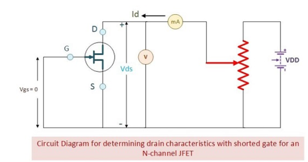
It clearly implies that the channel width is more as the width of depletion layer will not vary initially because there is no external reverse biasing. This allows a large magnitude of current to flow through the channel.
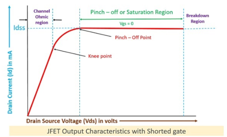
In this case, the N-type channel will simply behave as resistance region. The flow of current from drain to source will create the voltage drop between gate and source. This will eventually result in reverse biasing of the gate-source terminal. The reverse biasing will be more towards drain region that source region.
Terminologies involved in JFET characteristics
- Knee Point: There exists a point in the characteristics curve where the variation of drain current with drain-source voltage appears to be linear. But after this point, the linearity changes into a curve.
- Channel Ohmic Region: The region to the left of the knee point in the characteristics curve is the channel ohmic region.
- Pinch-off point: The point in the curve above which the drain current does not increases further no matter how much we are increasing the drain to source voltage, this point is termed as the pinch-off point.
- Pinch-off Voltage: The voltage at the pinch-off point is termed as pinch-off voltage because at this voltage the current is completely turned to be constant.
- Drain-Source Saturation Current: The drain to source saturation current is the current which becomes constant or completely enters a saturation state.
The region after the pinch-off point in the curve is termed as saturation region. When the JFET is allowed to work as an amplification device, the JFET utilizes this region for operation.
2. With external bias: When the external bias is applied to the gate-source terminal, the gate-source terminal becomes reversed bias externally. The pinch-off point is early as compared to the circuit which is not biased.
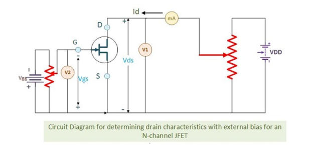
The different values of voltage give different values of current. Here the drain characteristics with respect to the variation in drain-source voltage is observed by keeping the gate-source voltage constant.
Transfer Characteristics
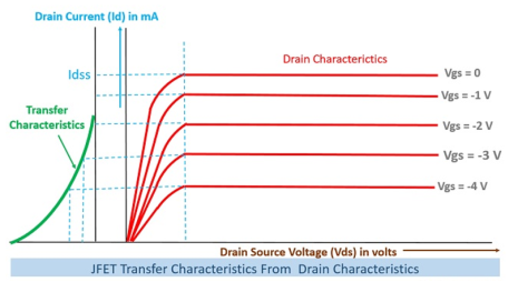
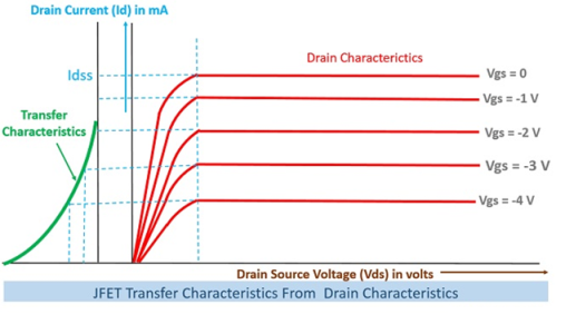
The transfer characteristics can be determined by observing different values of drain current with variation in gate-source voltage provided that the drain-source voltage should be constant. The transfer characteristics are just opposite to drain characteristics.
In transfer characteristics we are keeping the value of drain-source voltage constant.
The characteristic curve of transfer characteristics of JFET is shown below. It is observed that the value of drain current varies inversely with respect to gate-source voltage when the drain-source voltage is constant.
The input-output transfer characteristic of the JFET is not as straight forward as it is for the BJT.
In a BJT, β (hFE) defined the relationship between IB (input current) and IC (output current).
In a JFET, the relationship (Shockley’s Equation) between VGS (input voltage) and ID (output current) is used to define the transfer characteristics,
ID=IDSS(1−VGS/VP) ---------------------------(1)
As a result, FET’s are referred to a square law device
The FET is a three terminal device like the BJT, but operates by a different principle.
The three terminals are called the source, drain, and gate.
The voltage applied to the gate controls the current flowing in the source-drain channel.
No current flows through the gate electrode, thus the gate is essentially insulated from the source-drain channel.
Because no current flows through the gate, the input impedance of the FET is extremely large (in the range of 10^10...10^15 Ω)
MOSFETs are three terminal devices with a Gate, Drain and Source and both P-channel (PMOS) and N-channel (NMOS) MOSFETs are available. The main difference this time is that MOSFETs are available in two basic forms:
- Depletion Type – the transistor requires the Gate-Source voltage, ( VGS ) to switch the device “OFF”. The depletion mode MOSFET is equivalent to a “Normally Closed” switch.
- Enhancement Type – the transistor requires a Gate-Source voltage, ( VGS ) to switch the device “ON”. The enhancement mode MOSFET is equivalent to a “Normally Open” switch.
The symbols and basic construction for both configurations of MOSFETs are shown below.
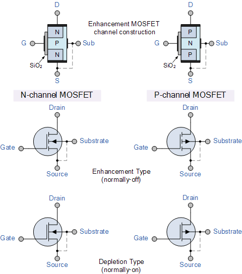
The four MOSFET symbols above show an additional terminal called the substrate and is not normally used as either an input or an output connection but instead it is used for grounding the substrate. It connects to the main semiconductive channel through a diode junction to the body or metal tab of the MOSFET.
The line in the MOSFET symbol between the drain (D) and source (S) connections represents the transistors semiconductive channel. If this channel line is a solid unbroken line then it represents a “Depletion” (normally-ON) type MOSFET as drain current can flow with zero gate biasing potential.
If the channel line is shown as a dotted or broken line, then it represents an “Enhancement” (normally-OFF) type MOSFET as zero drain current flows with zero gate potential. The direction of the arrow pointing to this channel line indicates whether the conductive channel is a P-type or an N-type semiconductor device.
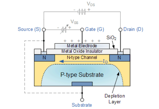
The construction of the Metal Oxide Semiconductor FET is different to that of the Junction FET.
Both the Depletion and Enhancement type MOSFETs use an electrical field produced by a gate voltage to alter the flow of charge carriers, electrons for n-channel or holes for P-channel, through the semi-conductive drain-source channel.
The gate electrode is placed on top of a very thin insulating layer and there are a pair of small n-type regions just under the drain and source electrodes.
With the insulated gate MOSFET device no such limitations apply so it is possible to bias the gate of a MOSFET in either polarity, positive (+ve) or negative (-ve).
This makes the MOSFET device especially valuable as electronic switches or to make logic gates because with no bias they are normally non-conducting and this high gate input resistance means that very little or no control current is needed as MOSFETs are voltage controlled devices.
Both the p-channel and the n-channel MOSFETs are available in two basic forms, the Enhancement type and the Depletion type.
Symbol
MOSFET : is another type of field effect transistor. The MOSFET has become one of the most important devices used in design and construction computers
MOSFET [metal oxide semiconductor field effect transistor]
Type of MOSFET
- Depletion type MOSFET
- Enhancement type MOSFET
- Power MOSFET
Enhancement type MOSFET : classified in to two type n. Channel or p. Channel E MOSFET
A) N-channel E MOSFET
B) P-channel E MOSFET
N-channel E MOSFET
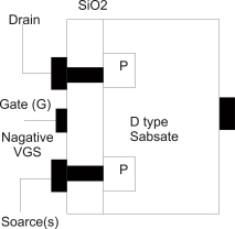
- A slab of P-type semiconductor is used as substrate. The substrate is sometimes connected to the source otherwise it is brought out as the fourth terminal.
- The drain and source terminal are connected to the n-type doped regions through the metallic contacts.
- The insulating sio2 layer is still present which isolates gate terminal from the substrate.
Effect of the insulting sio2 layer :
Due to the presence of the sio2 layer between gate terminal and n-type channel the i/p impedance of MOSFET is very high this is a desirable fracture of a MOSFET. Due to high i/p impedance the gate current IG= 0 for the d.c operating conditions.
Operation : the operation can be explained with two different operating
- Operation with VGS = 0
- Operation when VGS is +ve
1) Operating with VGS = 0 Volt
If VGS = 0 and a positive voltage is applied between its drain and source then due to the absence of the n-type channel a zero drain current will result.
2) Operation when Vgs Positive :
The positive potential at the gate terminal will repel the holes present in the p-type substrate.
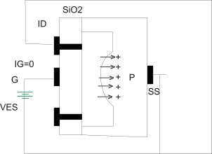
Formation of induced channel in n-channel enhancement MOSFET
This creates a depletion region near the sio2 insulating layer. But the minority carriers ie the electrons in the p-type substrate will be attracted towards the gate terminal and gather near the surface of sio2 as shown above
As we increase the positive VGS the number of e- gathering near the sio2 layer increases to such an extent that it creates an induced n-channel which connects the n-type doped regions.
The drain current then starts flowing through this induced channel. The value of VGS at which this conduction begins is called as the threshold Vtg. & is indicated.
Basic operating principle of SCR is understood by the two -transistor model of SCR, which is combination of p and n layers.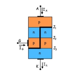
This is a pnpn thyristor. If we bisect it through the dotted line then we will get two transistors i.e. one pnp transistor with J1 and J2 junctions and another is with J2 and J3 junctions as shown in figure below.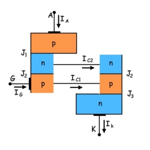
The relation between the collector current and emitter current is shown below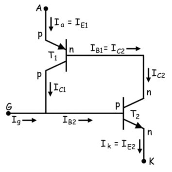
Here, IC is collector current, IE is emitter current, ICBO is forward leakage current, α is common base forward current gain and relationship between IC and IB is
Ic = β IB
Where, IB is base current and β is common emitter forward current gain.
For transistor T1
IC1 = α I a + I CB01 ------------------------------(i)
For transistor T2
IC2 = α 2 I k+ ICBo2 ---------------------------(ii) again Ic2 = β Ib2
Now, by the analysis of two transistors model we can get anode current,
Ia = Ic1 + Ic2 [applying KCL]
From equation (i) and (ii), we get,
Ia = α 1 Ia + ICB01 + α2 I K + I CB02 --------------------------------(iii)
If applied gate current is Ig then cathode current will be the summation of anode current and gate current i.e.
Ik = Ia + Ig
By substituting this value of Ik in (iii) we get,
Ia = α1 Ia + ICB01 + α2( I a + Ig) + I CB02
Ia = + α2 Ig + + ICB01 +I CB02/ 1 – (α1+α2)
From this relation we can assure that with increasing the value of  towards unity, corresponding anode current will increase.
Here is the explanation using two transistor model of SCR.
At the first stage when we apply a gate current Ig, it acts as base current of T2 transistor i.e. IB2 = Ig and emitter current of the T2 transistor IE2 = Ik.
Hence establishment of the emitter current gives rise α2 as
α 2 = ICB01 / Ig
Presence of base current will generate collector current as
Ic2 = β 2 x IB2 = β 2 I g
This IC2 is nothing but base current IB1 of transistor T1, which will cause the flow of collector current,
Ic2 = β 1 x IB1 = β1 β2 Ig
IC1 and IB1 lead to increase IC1 as Ia = Ic1 + I B1 and hence, α1 increases.
Now, new base current of T2 is Ig + Ic1 = (1 + β1β2) Ig , which will lead to increase emitter current Ik = Ia + Ic1 and as a result α2 also increases and this further increases Ic2 = β2(1 + β1β2) Ig .
.
As IB1 = Ic2 ,α 1 increases . This, continuous positive feedback effect increases
 towards unity and anode current tends to flow at high value. The value current then can only be controlled by external resistance of the circuit.
When connected to a direct current DC supply, the thyristor can be used as a DC switch to control larger DC currents and loads. When using the Thyristor as a switch it behaves like an electronic latch because once activated it remains in the “ON” state until manually reset. Consider the DC thyristor circuit below.
DC Thyristor Switching Circuit
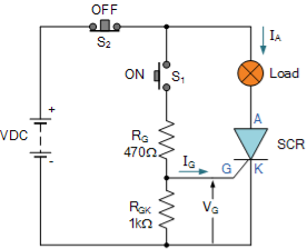
This simple “on-off” thyristor firing circuit uses the thyristor as a switch to control a lamp, but it could also be used as an on-off control circuit for a motor, heater or some other such DC load.
The thyristor is forward biased and is triggered into conduction by closing the normally-open “ON” push button, S1 which connects the Gate terminal to the DC supply via the Gate resistor, RG thus allowing current to flow into the Gate.
If the value of RG is set too high with respect to the supply voltage, the thyristor may not trigger. Once the circuit has been turned-“ON”, it self latches and stays “ON” even when the push button is released providing the load current is more than the thyristors latching current.
Additional operations of push button, S1 will have no effect on the circuits state as once “latched” the Gate loses all control. The thyristor is now turned fully “ON” (conducting) allowing full load circuit current to flow through the device in the forward direction and back to the battery supply.
One of the main advantages of using a thyristor as a switch in a DC circuit is that it has high current gain. The thyristor is a current operated device because a small Gate current can control a much larger Anode current.
The Gate-cathode resistor RGK is generally included to reduce the Gate’s sensitivity and increase its dv/dt capability thus preventing false triggering of the device.
As the thyristor has self -latched into the “ON” state, the circuit can only be reset by interrupting the power supply and reducing the Anode current to below the thyristors minimum holding current (IH) value.
Opening the normally-closed “OFF” push button, S2 breaks the circuit, reducing the circuit current flowing through the Thyristor to zero, thus forcing it to turn “OFF”
V-I characteristics:
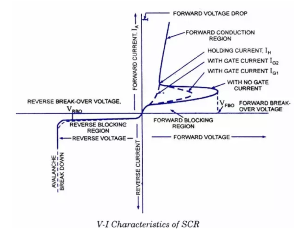
It is the curve between anode-cathode voltage (V) and anode current (I) of an SCR at constant gate current.
Figure shows the V-I characteristics of a typical SCR
Forward Characteristics
When anode is positive w.r.t. Cathode, the curve between V and I is called the forward characteristics.
The forward characteristics of SCR at IG=0.
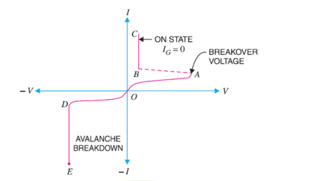
If the supply voltage is increased from zero, a point reached (point A) when the SCR starts conducting.
Under this condition , voltage across SCR suddenly drops as shown by dotted curve AB and most of supply voltage appears across the load resistance RL .
If proper gate current is made to flow, SCR can close at much smaller supply voltage.
Reverse Characteristics
When anode is negative w.r.t. Cathode, the curve between V and I is known as reverse characteristics.
The reverse voltage does come across SCR when it is operated with a.c. Supply.
If the reverse voltage is gradually increased, at first the anode current remains small (that is leakage current) and at some reverse voltage, avalanche breakdown occurs and the SCR starts conducting heavily in the reverse direction as shown by the curve DE.
This maximum reverse voltage at which SCR starts conducting heavily is known as reverse breakdown voltage.
The following terms are used in the characteristics of SCR :
- Breakover voltage
- Peak reverse voltage
- Holding current
- Forward current rating
- Circuit fusing rating
1. Breakover Voltage
- It is the minimum forward voltage, gate being open, at which SCR starts conducting heavily i.e. turned on.
- Thus, if the breakover voltage of an SCR is 200 V, it means that it can block a forward voltage (i.e. SCR remains open) as long as the supply voltage is less than 200 V. If the supply voltage is more than this value, then SCR will be turned on.
- In practice, the SCR is operated with supply voltage less than breakover voltage and it is then turned on by means of a small voltage applied to the gate.
- Commercially available SCRs have breakover voltages from about 50 V to 500 V.
2. Peak Reverse Voltage (PRV)
- It is the maximum reverse voltage (cathode positive w.r.t. anode) that can be applied to an SCR without conducting in the reverse direction.
- PRV is an important consideration while connecting an SCR in an a.c. Circuit. During the negative half of a.c. Supply, reverse voltage is applied across SCR. If PRV is exceeded, there may be avalanche breakdown and the SCR will be damaged if the external ciruit does not limit the current.
- Commercially available SCRS have PRV ratings upto 2.5 kV.
3. Holding Current
- It is the maximum anode current, gate being open, at which SCR is turned OFF from ON condition.
- When SCR is in the conducting state, it can not be turned OFF even if gate voltage is removed.
- The only way to turn off or open the SCR is to reduce the supply voltage to almost zero at which point the internal transistor comes out of saturation and opens the SCR.
- The anode current under this condition is very small (a few mA) and is called holding current.
- Thus, if an SCR has a holding current of 5mA, it means that if anode current is made less than 5 mA, then SCR will be turned off.
4. Forward Current Rating
- It is the maximum anode current that an SCR is capable of passing without destruction.
- Every SCR has a safe value of forward current which it can conduct. If the value of current exceeds this value, the SCR may be destroyed due to intensive heating at the junction.
- For example, if an SCR has a forward current rating of 40 A, it means that the SCR can safely carry only 40 A. Any attempt to exceed this value will result in the destruction of the SCR.
- Commercially available SCRs have forward current ratings from about 30A to 100A.
6. Circuit Fusing (I2t) Rating
It is the product of square forward surge current and the time of duration of the surge i.e.,
Circuit fusing rating =I2t
The circuit fusing rating indicates the maximum forward surge current capability of SCR.
For example, consider an SCR having circuit fusing rating of 90 A2s. If this rating is exceeded in the SCR circuit the device will be destroyed by excessive power dissipation.
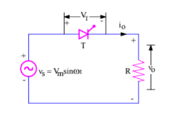
Let us understand the concept with the help of a simple circuit diagram as shown below.
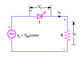
In the above circuit, a thyristor (or SCR) T is connected to load R and voltage source vs. This SCR will not conduct until and unless it is forward biased and gate signal is applied.
Application of gate signal is called firing.
During positive half cycle of supply voltage vs, the SCR is forward biased. If the thyristor T is fired (say at some phase angle α on the source voltage), it will become ON.
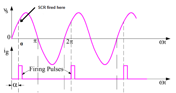
As SCR is now ON, it will start conducting. It will conduct from ωt = α to π.
Since load is resistive in nature, the load voltage v0 and load current i0 will follow the waveform of supply voltage.
The load voltage, load current and supply voltage waveforms are shown in figure below.
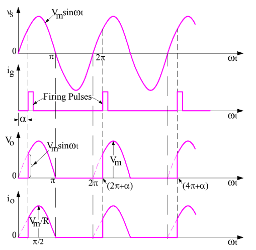
Compare the waveform of source voltage vs and load current i0. The SCR is getting turned ON at a phase angle of α. Thus, phase angle where thyristor T starts conducting is dependent on firing angle.
If firing angle α is 0 degree, then load current and source voltage will be in phase
If α is 90 degree then load current will start when the source voltage is maximum. Thus, the starting phase angle of load is controlled by firing angle..
At ωt= π, thyristor T will get commuated as the load current becomes zero and SCR is reversed biased from ωt = π to 2π.
This is known as Natural Commutation. We again need to fire SCR at (2π+α), (4π+α), (6π+α) and so on.
Advantage of Phase Control of SCR:
By having a phase control of SCR, we can have a control on output or load voltage. If the thyristor T is fired at α = 0 degree, the average load voltage would have been maximum as the SCR is ON for wt = 0 to π.
Similarly, if the firing angle α = π, the average load voltage would have been zero as SCR will not conduct at all.
Thus, by phase control of SCR, we can control the average load voltage.
References:
ELECTRONIC DEVICES AND CIRCUITS by VENKATA RAO, McGraw Hill
Getting started in Electronics by Forrest.M.Mims
All New Electronics – Self Teaching Guide by Harry Kybett & Earl Boysen
Practical Electronics for Inventors by Paul Scherz