Unit 3
Operational Amplifier and its applications
- It is commonly known as Op-amp.
- It requires an external power source hence is an active device.
- It is a versatile device that can be used to amplify ac as well as dc input signals.
- It can perform mathematical operations like addition, subtraction, multiplication, integration etc.
- Hence was named as Operational Amplifier due to its capability of performing mathematical operations.
- When external feedback is provided then the op-amp can be used as ac-dc signal amplifier, oscillator, regulator, active filter etc.
Input modes:
Single ended mode: If i/p sig is applied only to one of the i/p and other i/p terminal is connected to grid. OPAMP is said to be operating in the single ended mode.
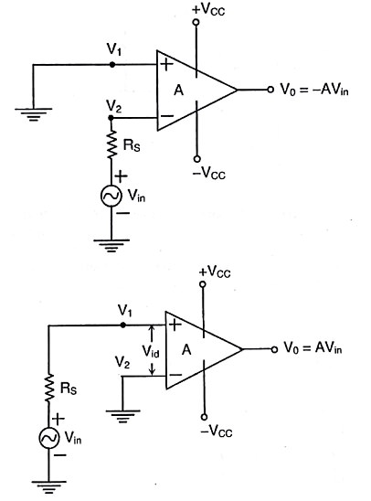
The i/p and o/p signal are 180 degree out of phase
If i/p is applied to inverting i/p
The i/p and o/p signals are in phase with each other
If i/p sig is applied to non- inverting i/p
Differential mode : In this, 2 opposite polarity last of phase sig are applied to the 2 i/ps of OP-AMP
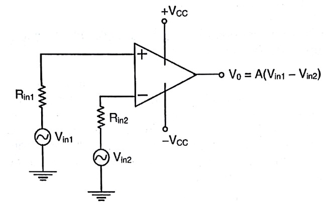
This type of operation is double ended operation. The difference between i/p sig is amplified appears at o/p.
Common mode: (CM)
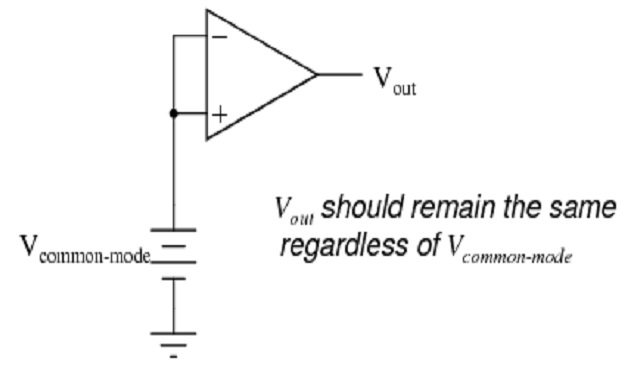
In CM, the same i/p signal is applied to both i/p terminals
Ideally o./p voltage should be produced by the OP-AMP.
Producing a zero o/p for a common mode signal is called as common mode rejection.
Common mode rejection radio (CMRR):
The signal which is present at both the i/p terminals of an OP – AMP is called as common mode signal.
The best e.g. Is “noise “. The OPAMP should produce a small o/p voltage corresponding to common mode signal. In other words, it should be capable of “rejecting” the common mode signal.
CMRR is the ability of differential amplifier to reject the common mode signal successfully. It is called as figure of merit of OP-AMP
Ideally, OP-AMP should produce very high gain for desired sig, i.e., single ended or differential signals.
The value of CMRR should be ideally infinite and practically as high as possible.
CMRR=Av/Acm
Av= open loop gain of OP-AMP
Acm= common mode gain of OP-AMP.
Open loop voltage gain is voltage gain of an OP-AMP in the open loop mode (without any feedback) of OP-AMP and it is very high.
In decibels, CMRR(dB)=20log10[Av/Acm]
CMMR stands for Common Mode Rejection Ratio defined as the ratio of differential voltage gain to common mode voltage gain
CMMR = Ad/Ac
Where Ad is Differential voltage gain
and Ac is common mode voltage gain
Let V1 and V2 be input voltages and Vo be output voltage
Being differential amplifier
Vo=V2-V1 .....(also known as differential output)
Common mode basically means that both the inputs are common to OpAmp
therefore, in our case V2=V1
so Vo becomes ZERO and thus
Common mode voltage gain is ZERO (for ideal OpAmp)
CMMR= Ad/Ac
Ac=0 (again, for ideal OpAMP)
Therefore, CMMR is infinite for ideal OpAmp
CMMR = 20 log CMRR is calculated in decibels
Eg-
if CMMR is 10000, then CMMR in db = 20log(10000)=80db
The input offset voltage is defined as the voltage that must be applied between the two input terminals of the op amp to obtain zero volts at the output.
Ideally the output of the op amp should be at zero volts when the inputs are grounded.
The input terminals are at slightly different dc potentials. VIO is represented by a voltage source that is in series with either the positive or negative input terminal (it is mathematically equivalent either way).
Input offset current:
Even though ideally the input currents of an op-amp is considered zero, in practice these NPN (or PNP) transistors of an input stage of op-amp do draw non-zero bias currents (IB1 & IB2). For input stage with a pair of NPN transistors, these bias currents IB1 and IB2 enter the input terminals of the op-amp and the difference between them (IB1-IB2) is referred as Input offset current.
If an input stage of an op-amp has exactly matching a pair of NPN transistors, then Input offset current will be zero. In actual, however, op-amps with transistor based input stage do have few nA of the input offset current and as low as few pA of input offset current for op-amps with JFET based input stage.
This is the current that flows in or out of the input pins. The input pins are the base pins of the transistor. In order for the input transistor to operate, the base current (IB) must flow. This base current is the input bias current. In actual use, when a resistor with a high resistance (RIN) is inserted at the input, the input bias current is used to express the input signal error.
For example, if RIN=1MΩ and IB=100nA, there is an error of 0.1 V. Therefore, when the impedance of the signal source is large, it is necessary to select a product with a small input bias current.
Note also that the difference between the bias current of the + and - input is the input offset current. Whether the bias current flows in or out differs depending on the input stage transistor.
An ideal op-amp has an infinite input impedance. Typically, the input impedance of a real op amp is many 100's of megaohms or more.
An ideal op-amp has an output impedance of zero ohms. Typically, the output impedance of a real op-amp is on the order of tens of ohms.
The slew rate of an op amp or any amplifier circuit is the rate of change in the output voltage caused by a step change on the input.
It is measured as a voltage change in a given time - typically V / µs or V / ms.
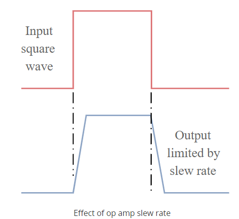
A typical general- purpose device may have a slew rate of 10 V / microsecond. This means that when a large step change is placed on the input, the electronic device would be able to provide an output 10 -volt change in one microsecond.
Op-amps are used in wide variety of applications:
- Voltage follower
- Selective inversion
- Current to voltage converter
- Active rectifier
- Integrator
- Voltage comparator.
Inverting amplifier
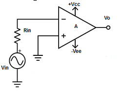
- As seen in the above figure, input is applied to only one terminal i.e. inverting input terminal.
- The other input terminal is supplied 0V i.e. grounded.
- Hence,
V1 = 0V and V2 = Vin
- Therefore output voltage Voutis given by,
Vout = A( - Vin )
Where, A is the voltage gain of op-amp.
- The negative sign implies that the output voltage is 1800 out of phase w.r.to the input voltage.
- Hence, the inverting amplifier amplifies the input signal by voltage gain A and inverts it at the output .
Non-Inverting Amplifier
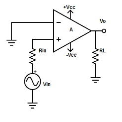
- As seen in the above figure, input is applied to only one terminal i.e. non-inverting input terminal.
- The other input terminal is supplied 0V i.e. grounded.
- Hence,
V1 = Vin and V2 = 0V
- Therefore output voltage Voutis given by,
Vout =AVin
Where, A is the voltage gain of op-amp.
- Here, the output voltage is more than the input voltage by voltage gain A and are also in phase with each other.
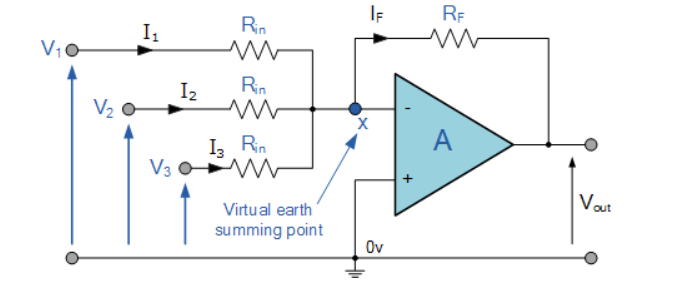
In this simple summing amplifier circuit, the output voltage, ( Vout ) now becomes proportional to the sum of the input voltages, V1, V2, V3, etc. Then we can modify the original equation for the inverting amplifier to take account of these new inputs thus:
IF = I1 + I2 + I3 = - [ V1/ Rin + V2 / Rin + V3/ Rin]
Inverting equation :
Vout = -Rf/ Rin x Vin
Then – Vout = [ Rf / Rin V1 + Rf/ Rin V2 + Rf/Rin V3]
Find the output voltage of the following circuit.
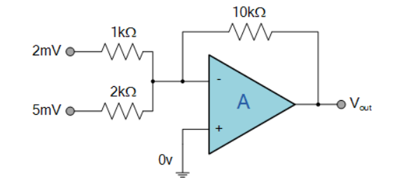
The gain of the circuit:
Gain(Av) = Vout/Vin = -Rf/Rin
We can now substitute the values of the resistors in the circuit as follows:
A1 = 10 K Ω/ 1kΩ = -10
A2 = 10KΩ/ 2kΩ = -5
The output voltage is the sum of the two amplified input signals and is calculated as:
Vout = (A1 x V1) x ( A2 x V2)
Vout = (-10(2mV)) + (-5(5mV)) = -45mV.
Then the output voltage of the Summing Amplifier circuit above is given as -45 mV and is negative as it is an inverting amplifier.
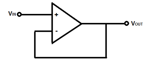
A voltage follower also called a unity-gain amplifier, a buffer amplifier, and an isolation amplifier is a op-amp circuit which has a voltage gain of 1.
This means that the op amp does not provide any amplification to the signal. The reason it is called a voltage follower is because the output voltage directly follows the input voltage, meaning the output voltage is the same as the input voltage.
Thus, for example, if 10V goes into the op amp as input, 10V comes out as output. A voltage follower acts as a buffer, providing no amplification or attenuation to the signal.
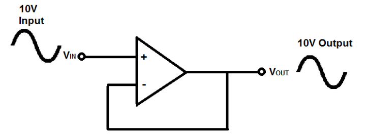
This high input impedance is the reason voltage followers are used. When a circuit has high input impedance, small current is drawn from the circuit.
In ohm's law, current, I=V/R. Thus, the greater the resistance, the less current is drawn from a power source. Thus, the power of the circuit does not affect when current is feeding a high impedance load.
The below circuit is a circuit in which a power source feeds a low-impedance load.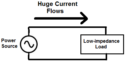
In this circuit above, the load demands and draws a huge amount of current, because the load is low impedance. According to ohm's law, again, current, I=V/R. If a load has too low resistance, it draws huge amounts of current. This causes huge amounts of power to be drawn from the power source and, because of this, causes high disturbances and use of the power source powering the load.
Now let's look at the circuit below, connected to an op-amp voltage follower:
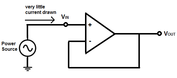
This circuit above now draws less current from the power source above. Because the op amp has such high impedance, it draws less current. And because op amp has no feedback resistors it gives the same output, the circuit outputs the same signal that is fed in.
This is one of the reasons voltage followers are used. They draw little current, not disturbing the original circuit, and give the same voltage signal as output. They act as isolation buffers, isolating a circuit so that the power of the circuit is disturbed too little.
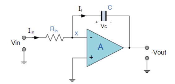
Op-amp Integrator is an operational amplifier circuit that performs the mathematical operation of Integration, that is we can cause the output to respond to changes in the input voltage over time as the op-amp integrator produces an output voltage which is proportional to the integral of the input voltage.
When a step voltage, Vin is firstly applied to the input of an integrating amplifier, the uncharged capacitor C has very little resistance and acts a bit like a short circuit allowing maximum current to flow via the input resistor, Rin as potential difference exists between the two plates.
No current flows into the amplifiers input and point X is a virtual earth resulting in zero output.
As the impedance of the capacitor at this point is too low, the gain ratio of XC/RIN is also very small giving an overall voltage gain of less than one, voltage follower circuit).
As the feedback capacitor, C begins to charge up due to the influence of the input voltage, its impedance Xc slowly increase in proportion to its rate of charge. The capacitor charges up at a rate determined by the RC time constant, ( τ ) of the series RC network.
Negative feedback forces the op-amp to produce an output voltage that maintains a virtual earth at the op-amp’s inverting input.
Since the capacitor is connected between the op-amp’s inverting input (which is at virtual ground potential) and the op-amp’s output (which is now negative), the potential voltage, Vc developed across the capacitor slowly increases causing the charging current to decrease as the impedance of the capacitor increases.
This results in the ratio of Xc/Rin increasing producing a linearly increasing ramp output voltage that continues to increase until the capacitor is fully charged.
At this point the capacitor acts as an open circuit, blocking any more flow of DC current.
The ratio of feedback capacitor to input resistor ( XC/RIN ) is now infinite resulting in infinite gain. The result of this high gain is that the output of the amplifier goes into saturation as shown below.
Saturation occurs when the output voltage of the amplifier swings heavily to one voltage supply rail or the other with little or no control in between.
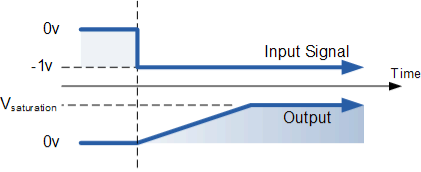
The rate at which the output voltage increases the rate of change is determined by the value of the resistor and the capacitor, “RC time constant“.
By changing this RC time constant value, either by changing the value of the Capacitor, C or the Resistor, R, the time in which it takes the output voltage to reach saturation can also be changed for example.
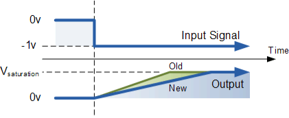
If we apply a constantly changing input signal such as a square wave to the input of an Integrator Amplifier then the capacitor will charge and discharge in response to changes in the input signal. This results in the output signal being that of a sawtooth waveform whose output is affected by the RC time constant of the resistor/capacitor combination because at higher frequencies, the capacitor has less time to fully charge.
A differentiator circuit is one in which the voltage output is directly proportional to the rate of change of the input voltage with respect to time.
This means that a fast change to the input voltage signal, the greater the output voltage change in response.
As a differentiator circuit has an output that is proportional to the input change, some of the standard waveforms such as sine waves, square waves and triangular waves provide different waveforms at the output of the differentiator circuit.
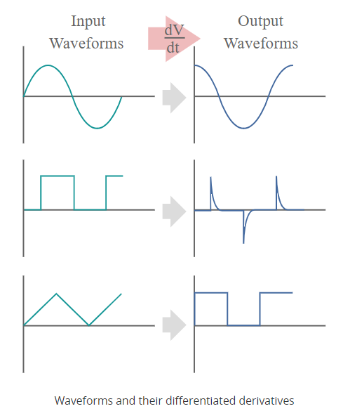
For these waveforms it is seen that the greater the rate of change of the waveform at the input, the higher the output voltage at that point.
For the square wave input, only very short spikes are seen. The spikes will be limited by the slope of the edges of the input waveform and also the maximum output of the circuit and its slew rate and bandwidth.
The spikes should also decay swiftly. Again, this may be limited by the circuit and on the diagram, the decay is not shown to be infinitely fas, representing better what a real- life waveform may look like.
The triangular wave input transforms to a square wave in line with the rising and falling levels of the input waveform.
In its basic form the center of the circuit is based around the operational amplifier itself. In addition to this a couple of other electronics components are required: a capacitor is connected from the input of the whole circuit to the inverting input of the operational amplifier. A feedback resistor is then used to provide the negative feedback around the op amp chip - this is connected from the output of the operational amplifier to its inverting input.
The non-inverting input is connected to ground.
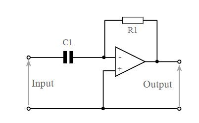
The differentiator circuit is given by
Vout = - R C dVin/dt
Where:
Vout = output voltage from op amp differentiator
Vin = input voltage
t = time in seconds
R = resistor value in the differentiator in Ω
C = capacitance of differentiator capacitor in Farads
dVin/dt = rate of change of voltage with time.
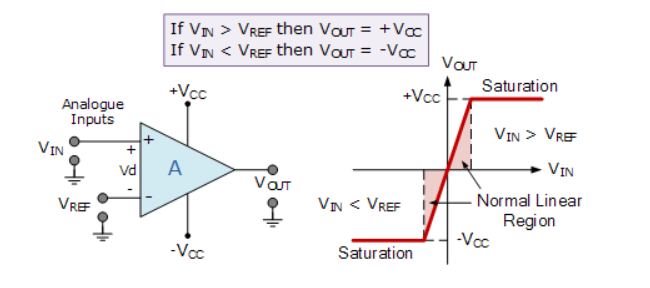
- The op-amp voltage comparator compares the magnitudes of two voltage inputs and determines which is the largest of the two.
- Consider the basic op-amp voltage comparator circuit below.
- First assume that VIN is less than the DC voltage level at VREF, ( VIN < VREF ). As the non-inverting (positive) input of the comparator is less than the inverting (negative) input, the output will be LOW and at the negative supply voltage, -Vcc resulting in a negative saturation of the output.
- If we now increase the input voltage, VIN so that its value is greater than the reference voltage VREF on the inverting input, the output voltage rapidly switches HIGH towards the positive supply voltage, +Vcc resulting in a positive saturation of the output.
- If we reduce again the input voltage VIN, so that it is slightly less than the reference voltage, the op-amp’s output switches back to its negative saturation voltage acting as a threshold detector.
- Thus the op-amp voltage comparator is a device whose output is dependent on the value of the input voltage, VIN with respect to some DC voltage level as the output is HIGH when the voltage on the non-inverting input is greater than the voltage on the inverting input, and LOW when the non-inverting input is less than the inverting input voltage.
- This condition is true regardless of whether the input signal is connected to the inverting or the non-inverting input of the comparator.
- The output voltage is completely dependent on the op-amps power supply voltage. In theory due to the op-amps high open-loop gain the magnitude of its output voltage could be infinite in both directions, (±∞).
- However practically, and for obvious reasons it is limited by the op-amps supply rails giving VOUT = +Vcc or VOUT = -Vcc.
- The basic op-amp comparator produces a positive or negative voltage output by comparing its input voltage against some preset DC reference voltage.
- Generally, a resistive voltage divider is used to set the input reference voltage of a comparator, but a battery source, zener diode or potentiometer for a variable reference voltage can all be used as shown.
References:
ELECTRONIC DEVICES AND CIRCUITS by VENKATA RAO, McGraw Hill
Getting started in Electronics by Forrest.M.Mims
All New Electronics – Self Teaching Guide by Harry Kybett & Earl Boysen
Practical Electronics for Inventors by Paul Scherz
