Unit 4
BJT
*BJT:-The BJT is constructed with the three draped semiconductors region’s separate by two Pn junctions as shown below
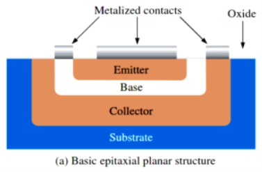
-Basic epitaxial planner structures.
-Three terminal with region’s are called emitter, base and collector.
-The physical representation of the two types of BJT’s,
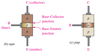
One type consists between two regions separated by a P region (npn) and other type consists of two p regions separated by an n region (pnp).
-The Pn junction joining the base region and the emitter region is called the base emitter junction.
-The Pn junction joining the base region and the collector region is called the base collector junction.
-The base region is lightly doped and very thin compared to the heavily doped emitter and the moderately doped collector regions.
*Base Transistor Operation:-
In order for the transistor to operate properly as an amplifier the two pn junction must be correctly biased with the external D.C vtg.
-The next figure shows the proper bias arrangement for both the npn and pnp transistors for active operation as an amplifier.
-In both the cases the base emitter
(BE) junction is forward biased & the base collector junction (BC) junction is reverse biased
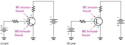
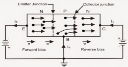
- As from above figure consider n-p-n transistor. The forward bias from base to emitter narrow’s the BE depletion region and the reverse bias from base to collector widens the BC depletion region shown in figure.
- The heavily doped N-TYPE emitter region is full with conduction band(frep) electron’s that easily diffuse through the forward biased BE junction into the p-type base region where they become minority carrier’s same as forward biased diode region
- The base region is lightly doped & very thin so that it has a very limited number of holes.
- Those only a small percentage of all the e-flowing the BE junction can combine with the available holes in the base.
- The relatively few recombined flow out of the base lead as valance electrons, forming as small base current.
- Most of the e flowing from the emitter into the thin lightly dooped base region do not recombine but diffuse into the BC depletion region.
- The BC depletion region diffuse e is being pulled across the reverse biased BC junction by the attraction of the collector supply vtg.
- The electrons now move through the collector region, out through the collector lead into the +ve terminal of the collector vtg source. This forms the collector electrons current.
- The collector current is much larger than the base current.
- This is the reason transistor exhibit current gain.
Common Emitter (CE) configuration
The important points about the CE
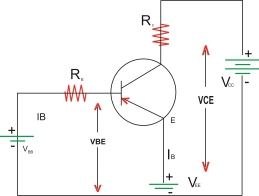
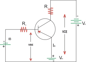
Configurations are as follows: the emitter acts as a common terminal between I/p and output. The /p Vtg. Is called between base and emitter
Hence VBE is the I/p Vtg. And IB is the input current.
The O/p is taken between the collector and emitter. There for VCE is the O/p Vtg. And IC is the O/p current.
In order to operate the transistor in its active region the base emitter (BE) junction is forward biased and collector base junction is reverse biased.
- Current relations in CE Configuration:
IE = IC + IB
Where IC =  d.c.IE + ICBO
Rearrange this eqn to get
IC – ICBO =  d.c.IE
 -
-  = IE = IC + IB
 ] = IB -
IC  ] = IB +
 ] +
] + 
- Current gain
 : as
: as  is the ration of o/p current TC and I/p current IB it called common emitter current amplification factor or simply current gain. Thus transistor acts as current amplifier.
The value of  is match higher than
 =
= 
 =
=  =
=  =
= 
IC =  IB +
IB +  …….. I
But  =
= 
 1 +
1 +  =
=  + 1
+ 1
1 +  =
= 
 1 +
1 +  =
= 
Put in eqn I
IC =  IB + (1+
 ICBO above eqn can be expressed as
IC =  IB + ICEO
Where ICEO is the reverse saturation current for the CE configuration which is given by
ICEO = (1+  ) ICBO
- Reverse leakage current :
The Reverse leakage current of a transistor operating
In the LE configuration is denoted by
ICEO = (1 +  ) ICBO
As the value of 
- Match greater than 1 ICEO >>>> ICBO
- As IC =

Put IB = 0
 IC = (1 +
The Reverse leakage current (ICEO)
Increases with increase in the temperature this current flows in the same direction as that of IC there for the collector current IC will increase with increase in temperature even when IB is constant
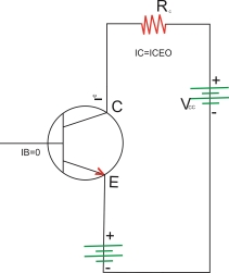
This is called as thermal instability so in CE configuration thermal stabilizing CKT must be included.
- Relation between IC and IB (Current gain
 )
)
We know that
IC 
Though ICEO is large it is much smaller as compared to . Therefor the eqn for IC gets modified as
 C =
C = 

- Relation betn
 &
& :
:
We know that
 but
but
 =
=  =
= 
 =
= 
Similarly we can obtain the expression for  d.c in terms of
  as follows
 d.c =
d.c =  but
but 
=
Multiply & divide numerator & denominator for by IE
 d.c =
d.c = 
 d.c =
d.c = 
 =
= 
- Impact characteristics :
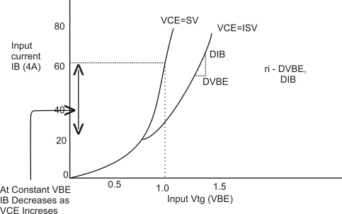
The value of dynamic input resistance ri is low for the CE configuration but it is not as low as that of CE configuration
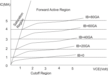
- Cutoff region: Both the BE & CB junctions are reverse biased to operate the transistor in cutoff region. The base current IB = 0 & the collector current is equal to the reverse leakage ICEO. The region below the characteristics for
IB = 0 is cutoff region.
- Active region : the BE emitter junction is forward biased CB junction is reverse biased to operate the transistor in the active region
The collector current IC increases slightly with increase in the vtg.VCE. However the collector current is largely dependent on the base current IB
At fixed value of VCE if IB is increased then it will cause IC to increase substantially.
This is because IC = BIB this relation is true only for the active region of operation.
- Saturation region : the BE junction as well as the collector junction must be forward biased to operate the transistor in its saturation region
- Dynamic o/p resistance
 / constant IB
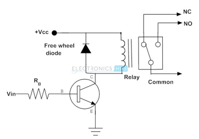
a power circuit using a relay
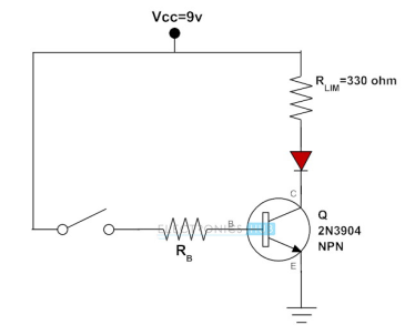
Transistor to Switch the LED
- When the switch at the base terminal is open, no current flows through the base so the transistor is in the cut-off state. Therefore, the circuit acts as open-circuit and the LED becomes OFF.
- When the switch is closed, base current starts flowing through the transistor and then drives into saturation results to LED become ON.
- Resistors are placed to limit the currents through the base and LED. It is also possible to vary the intensity of LED by varying the resistance in the base current path.
Transistor to Operate the Relay
- Consider the below circuit to know the operation of a transistor to energize the relay coil. The input applied at the base causes to drive the transistor into saturation region, which further results the circuit becomes short circuit. So, the relay coil gets energized and relay contacts get operated.
- In inductive loads, particularly switching of motors and inductors, sudden removal of power can keep a high potential across the coil.
- This high voltage can cause considerable damage to the rest circuit. Therefore, use the diode in parallel with inductive load to protect the circuit from induced voltages of the inductive load.
Feedback Amplifier is a device that is based on the principle of feedback. The process by which some part or fraction of output is combined with the input is known as feedback.
Feedback amplifiers are the type of amplifiers in which a part of the output is given back to the input.
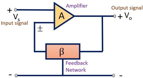
Amplifier is a device that amplifies the signal. In an ideal amplifier, there exist some important characteristics like voltage gain, input impedance, output impedance, bandwidth etc.
These parameters of an amplifier are controlled by employing a feedback network. Thus, a feedback network is employed in an amplifier to control the gain and other factors of the device.
Positive Feedback amplifier– It is a type of an amplifier in which source signal and the feedback signal are in the same phase. Thus, the feedback signal applied increases the strength of the input signal.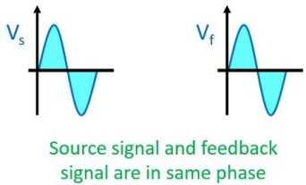
Negative Feedback amplifier– In this type of amplifier source signal and the feedback signal are out of phase with each other. Thus, the feedback signal applied to decrease the strength of the input signal.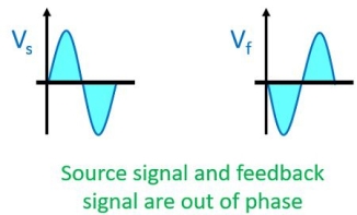

An input signal Vs is applied to the amplifier with gain A, that produces an amplified signal, Vo.
A portion or fraction of this Vo is then fed to a feedback network having gain β. The output of feedback network is Vf, this signal is then given to summer or a mixer that resultantly produces either sum or difference of two signal depending on their phase relationship.
The gain of an amplifier is given as the ratio of output voltage or current to the input voltage or current.
The gain of the circuit without feedback is given as
A= Vo/Vd -----------------(1)
The gain of feedback network is given as
β = Vf/Vo ----------------(2)
Vd is the mixer output voltage given by
Vd = Vs ± Vf --------------------------(3)
The signal voltage Vs and mixer output voltage Vd will only be equal in a feedback amplifier unless the output is not generated.
From Eq 1 we can write as
Vo = A Vd -----------------------------------(4)
Substituting the value Vd in eq 4
Vo = A[ Vs ± Vf] -------------------------------(5)
From Eq 2
Vf = β Vo ------------------------------------(6)
Substituting the value of Vf in eq 5
Vo = A[ Vs ± β Vo]
Vo = A Vs ± A β Vo
Vo ± A β Vo = A Vs
Vo[1± Aβ] = A Vs
Vo/Vs = A / 1 ± Aβ
Avf = A/ 1 ± Aβ where Vo/Vs = Avf
This is the desired value for the gain of the feedback amplifier.
The gain of an amplifier is always greater than 1. This simply means that some elements are present which increases the gain of the amplifier. That element can be a transistor or a MOSFET.
But a feedback network is always a linear network consisting of RLC elements and it does not contain any such amplification device.
That’s why the value of Vf is always less than Vo.
So,β < 1
In case of a positive feedback the source signal will be in phase with that of the feedback signal.
Thus, the mixer will produce the summation of the two signal applied to it in case of positive feedback.
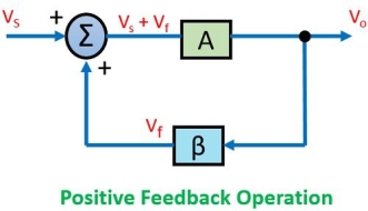
So, the gain of the amplifier is given as
Avf = A/ 1 - Aβ
This is the gain for a positive feedback amplifier.
The source signal and the feedback signal are out of phase with respect to each other.
Thus, the mixer circuit will resultantly produce the difference between the two signal in case of a negative feedback amplifier.
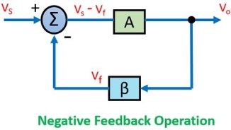
So, in this case, the gain of the amplifier is given as
Avf = A / 1+Aβ
For a negative feedback, the value of denominator is always greater than 1, this will decrease the overall gain of the system by the factor 1 +Aβ.
In case of a positive feedback system, the value of denominator is always less than 1, this will resultantly increase the overall gain by 1 – Aβ.
Gain Stability Relation
For an ideal system, the gain of the amplifier is infinite. Thus, for a smaller input, we will have a much higher value as output. So, such a large gain is not desirable in the circuit.
The system becomes stable only when its gain is small.
Hence, by decreasing the gain the stability of the system increases and vice-versa.
So, to have a stable system, the gain of the amplifier must be small and it is achieved by employing negative feedback in the circuit.
Principle:
A feedback amplifier generally consists of two parts. They are the amplifier and the feedback circuit. The feedback circuit usually consists of resistors. The concept of feedback amplifier can be understood from the following figure.
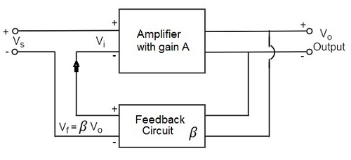
From the above figure, the gain of the amplifier is represented as A. The gain of the amplifier is the ratio of output voltage Vo to the input voltage Vi. The feedback network extracts a voltage Vf = β Vo from the output Vo of the amplifier.
This voltage is added for positive feedback and subtracted for negative feedback, from the signal voltage Vs. Now,
Vi=Vs+Vf=Vs+βVoVi
Vi=Vs−Vf=Vs−βVoVi
The quantity β = Vf/Vo is called as feedback ratio or feedback fraction.
Positive:
The feedback in which the feedback energy i.e., either voltage or current is in phase with the input signal and thus aids it is called as Positive feedback.
Both the input signal and feedback signal introduces a phase shift of 180o thus making a 360o resultant phase shift around the loop, to be finally in phase with the input signal.
Though the positive feedback increases the gain of the amplifier, it has the disadvantages such as
- Increasing distortion
- Instability
It is because of these disadvantages the positive feedback is not recommended for the amplifiers. If the positive feedback is sufficiently large, it leads to oscillations, by which oscillator circuits are formed.
Negative Feedback
The feedback in which the feedback energy i.e., either voltage or current is out of phase with the input and thus opposes it, is called as negative feedback.
In negative feedback, the amplifier introduces a phase shift of 180o into the circuit while the feedback network is so designed that it produces no phase shift or zero phase shift. Thus, the resultant feedback voltage Vf is 180o out of phase with the input signal Vin.
Though the gain of negative feedback amplifier is reduced, there are many advantages of negative feedback such as
- Stability of gain is improved
- Reduction in distortion
- Reduction in noise
- Increase in input impedance
- Decrease in output impedance
- Increase in the range of uniform application
In a negative feedback amplifier, a small portion of the output voltage is fed back to the input. When the feedback voltage is applied in series with the signal voltage, the arrangement is Voltage Series Negative Feedback Amplifier.
The instantaneous polarity of the feedback voltage is normally opposite to the signal voltage polarity. So, the feedback voltage is negative with respect to the signal voltage, hence the term negative feedback.

Negative feed back amplifier feedback network
An amplifier with two input terminals and one output is shown in triangular representation. The amplifier has a voltage gain (Av), and its output voltage (vo) is applied to a feedback network that reduces vo by a factor (B) to produce a feedback voltage (vf).
The feedback network may be as simple as the resistive voltage divider shown in Fig. b. At the amplifier input, the instantaneous level of vf is applied negative with respect to vs, so that the amplifier input terminal voltage is,
Vi=vs-vf
Because the amplifier input voltage is lower than the signal voltage, the output voltage is lower than that produced when negative feedback is not used.
This means the overall voltage gain (vo/vi) is reduced by negative feedback.
Any signals traveling around the feedback loop are multiplied by A then β. Aβ is the “loop” gain.
If Aβ is less than unity at the high frequencies the phase shift reaches 180 o the high frequency phase shifted signal will gradually fade away instead of progressively building into major oscillations.
If Aβ is greater than unity, the sine waves will build upon each other every time they go through the loop, and their amplitude gradually increases because Aβ is amplifying them.
A feedback amplifier generally consists of two parts. They are the amplifier and the feedback circuit. The feedback circuit usually consists of resistors. The concept of feedback amplifier can be understood from the following figure below.
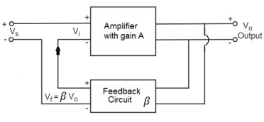
From the above figure, the gain of the amplifier is represented as A. The gain of the amplifier is the ratio of output voltage Vo to the input voltage Vi. The feedback network extracts a voltage Vf = β Vo from the output Vo of the amplifier.
This voltage is added for positive feedback and subtracted for negative feedback, from the signal voltage Vs.
So, for a positive feedback,
Vi = Vs + Vf = Vs + β Vo
The quantity β = Vf/Vo is called as feedback ratio or feedback fraction.
The output Vo must be equal to the input voltage (Vs + βVo) multiplied by the gain A of the amplifier.
Hence,
(Vs+βVo)A=Vo
Or
AVs+AβVo= Vo
Or
AVs=Vo(1−Aβ)AVs
Therefore
Vo/Vs=A/1−Aβ
Let Af be the overall gain (gain with the feedback) of the amplifier. This is defined as the ratio of output voltage Vo to the applied signal voltage Vs, i.e.,
Af=OutputVoltage/InputSignalVoltage=Vo/Vs
From the above two equations, the gain of the feedback amplifier with positive feedback is given by
Af=A/1−Aβ
Where Aβ is the feedback factor or the loop gain.
If Aβ = 1, Af = ∞. Thus, the gain becomes infinity, i.e., there is output without any input. In another words, the amplifier works as an Oscillator.
The condition Aβ = 1 is called as Barkhausen Criterion of oscillations.
RC phase-shift oscillators use resistor-capacitor (RC) network as shown in Figure 1 to provide the phase-shift required by the feedback signal. They have excellent frequency stability and can yield a pure sine wave for a wide range of loads.
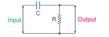
Ideally a simple RC network is expected to have an output which leads the input by 90o.The phase-difference will be less than this as the capacitor used in the circuit cannot be ideal.
Mathematically the phase angle of the RC network is expressed as
ɸ = tan -1 Xc / R
where, XC = 1/(2πfC) is the reactance of the capacitor C and R is the resistor. In oscillators, these kind of RC phase-shift networks, each offering a definite phase-shift can be cascaded to satisfy the phase-shift condition led by the Barkhausen Criterion.
RC phase-shift oscillator is formed by cascading three RC phase-shift networks, each offering a phase-shift of 60o, as shown by Figure
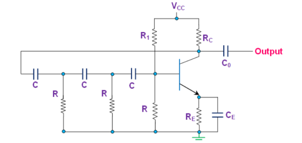
- The collector resistor RC limits the collector current of the transistor , resistors R1 and R form the voltage divider network while the emitter resistor RE improves the stability.
- The capacitors CE and Co are the emitter by-pass capacitor and the output DC decoupling capacitor, respectively.
- Further, the circuit also shows three RC networks employed in the feedback path. This, arrangement causes the output waveform to shift by 180o during its course of travel from output terminal to the base of the transistor.
- The signal will be shifted again by 180o by the transistor in the circuit due to the phase-difference between the input and the output will be 180o in the case of common emitter configuration.
- This makes the net phase-difference to be 360o, satisfying the phase-difference condition.
The generalized expression for the frequency of oscillations produced by a RC phase-shift oscillator is given by
f=1/ 2π RC  N
N
where, N is the number of RC stages formed by the resistor R and the capacitors C.
A Wien-Bridge Oscillator is a type of phase shift oscillator which is based upon a Wien-Bridge network (Figure) comprising of four arms connected in a bridge fashion.
Here two arms are purely resistive while the other two arms are a combination of resistors and capacitors.
One arm has resistor and capacitor connected in series (R1 and C1) while the other has them in parallel (R2 and C2).
This indicates that these two arms of the network behave identical to that of high pass filter or low pass filter.
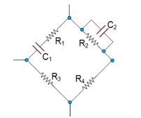 Wein bridge network
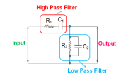 Two arms of wein bridge network
At high frequencies, the reactance of the capacitors C1 and C2 will be much less due to which the voltage V0 will become zero as R2 will be shorted. Next, at low frequencies, the reactance of the capacitors C1 and C2 will become very high.
However, the output voltage V0 will remain at zero only, as the capacitor C1 would be acting as an open circuit. This kind of behavior exhibited by the Wien-Bridge network makes it a lead-lag circuit in the case of low and high frequencies, respectively.
Amidst these two high and low frequencies, there exists a particular frequency at which the values of the resistance and the capacitive reactance will become equal to each other, producing the maximum output voltage. This frequency is referred to as resonant frequency. The resonant frequency for a Wein Bridge Oscillator is calculated using the following formula:
f r = 1/ 2π  C1 R2 C2
If R1 = R2 =R and C1=C2=C
Fr = 1/ 2π RC
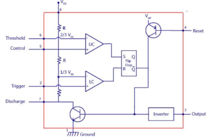
For 555 timer working as a flip flop or as a multi-vibrator, it has a particular set of configurations. Some of the major features include :
- It operates from a wide range of power ranging from +5 Volts to +18 Volts supply voltage.
- Sinking or sourcing 200 mA of load current.
- The external components should be selected properly so that the timing intervals can be made into several minutes along with the frequencies exceeding several hundred kilohertz.
- The output of a 555 timer can drive a transistor-transistor logic (TTL) due to its high current output.
- It has a temperature stability of 50 parts per million (ppm) per degree Celsius change in temperature which is equivalent to 0.005 %/ °C.
- The duty cycle of the timer is adjustable.
- Also, the maximum power dissipation per package is 600 mW and its trigger and reset inputs has logic compatibility.
The 555 generally operates in 3 modes:
- A-stable
- Mono-stable
- Bi-stable modes.
Astable mode
This means there will be no stable level at the output. So, the output will be swinging between high and low. This character of unstable output is used as a clock or square wave output for many applications.
Mono-stable mode
This configuration consists of one stable and one unstable state. The stable state can be chosen either high or low by the user.
If the stable output is set at high (1), the output of the timer is high (1). At the application of an interrupt, the timer output turns low (0). Since the low state is unstable it goes to high (1) automatically after the interrupt passes.
Bi-stable mode
In bi-stable mode, both the output states are stable. At each interrupt, the output changes from low (0) to high (1) and vice versa and stays there.
For example, if we have a high (1) output, it will go low(0) once it receives an interrupt and stays low (0) till the next interrupt changes the status.
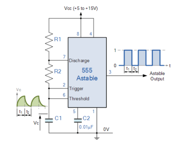
In the 555 Oscillator circuit above, pin 2 and pin 6 are connected allowing the circuit to re-trigger itself on each and every cycle allowing it to operate as a free running oscillator.
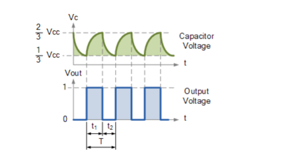
During each cycle capacitor, C charges up through both timing resistors, R1 and R2 but discharges itself only through resistor, R2 as the other side of R2 is connected to the discharge terminal, pin 7.
Then the capacitor charges up to 2/3Vcc which is determined by 0.693(R1+R2)C combination and discharges itself down to 1/3Vcc (the lower comparator limit) determined by the 0.693(R2*C) combination.
This results in an output waveform whose voltage level is approximately equal to Vcc – 1.5V and whose output “ON” and “OFF” time periods are determined by the capacitor and resistors combinations.
The individual times required to complete one charge and discharge cycle of the output is therefore given as:
t 1 = 0.693 (R1 + R2). C and
t 2 = 0.693 x R2 x C
Where, R is in Ω and C in Farads.
T = t1 + t2 = 0.693 (R1 + 2 R2) . C
f = 1/T = 1.44/ (R1 + 2 R2) . C
Duty Cycle = TON / TOFF + TON = R1 + R2 / (R1 + 2R2) %
Problem :
An Astable 555 Oscillator is constructed using the following components, R1 = 1kΩ, R2 = 2kΩ and capacitor C = 10uF. Calculate the output frequency from the 555 oscillator and the duty cycle of the output waveform.
t1 – capacitor charge “ON” time is calculated as:
t1 = 0.693(R1 + R2). C
= 0.693(1000 +2000) x 10 x 10 -6 = 0.021 s= 0.21 ms
t2 – capacitor discharge “OFF” time is calculated as:
t2 = 0.693 R2. C
= 0.693 X 2000 x 10 x 10 -6 = 14ms
Total periodic time ( T ) is therefore calculated as:
T = t1 + t2 = 21 ms + 14 ms = 35 ms.
The output frequency, ƒ is therefore given as:
f = 1/T = 1/35ms = 28.6 Hz
Giving a duty cycle value of:
Duty Cycle = R1 + R2 / (R1 + 2 R2) = 1000 + 2000/ (1000 + 2 x 2000) = 60%
References:
ELECTRONIC DEVICES AND CIRCUITS by VENKATA RAO, McGraw Hill
Getting started in Electronics by Forrest.M.Mims
All New Electronics – Self Teaching Guide by Harry Kybett & Earl Boysen
Practical Electronics for Inventors by Paul Scherz