Unit 5
Digital Electronics Fundamentals
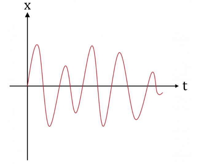
- An analog signal is one type of continuous time-varying signals, and these are classified into composite and simple signals.
- A simple type of analog signal is nothing but a sine wave, and that can’t be decomposed, whereas a composite type analog signal can be decomposed into numerous sine waves.
- An analog signal can be defined by using amplitude, time period otherwise frequency, & phase. Amplitude streaks the highest height of the signal, frequency streaks the rate at which an analog signal is varying, and phase streaks the signal position with respect to time nothing.
- An analog signal is not resistant toward the noise, therefore; it faces distortion as well as reduces the transmission quality. The analog signal value range cannot be fixed.
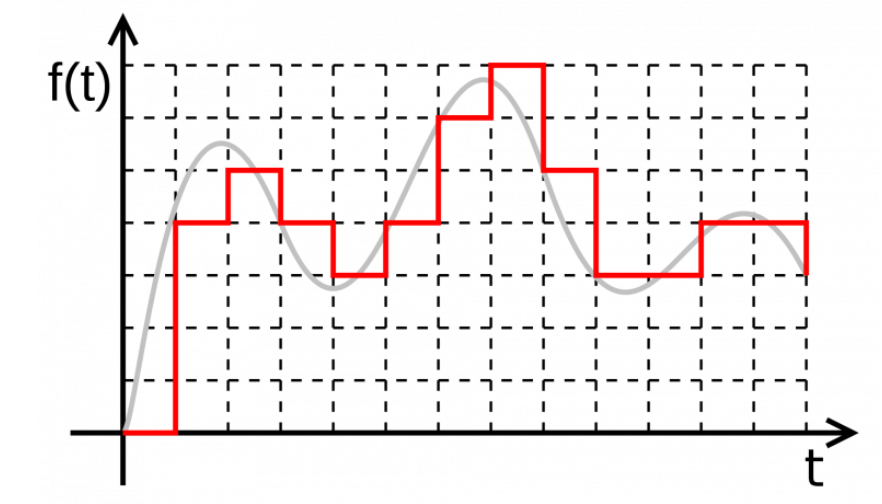
- Digital signals carry the data although it is a bit different. These signals are discrete or not continuous.
- A digital signal carries the data in the form of binary because it signifies in the bits. These signals can be decomposed into sine waves which are termed as harmonics. Every digital signal has amplitude, frequency, & phase like the analog signal.
- This signal can be defined by bit interval as well as bit rate. Here, bit interval in nothing but the required time for transmitting an only bit, whereas the bit rate is bit interval frequency.
Introduction to number system and conversions
A digital system understands positional number system where there are few symbols called digits and these symbol represents different values depending on their position in the number.
A value of the digit is determined by using
- The digit
- Its position
- The base of the number system
- It uses two digits 0 and 1.
- It is also called as base 2 number system.
- Here, each position in any binary number represents a power of the base (2). Example: 23
- The last position represents a y power of the base (2). Example: 2y where y represents the last position.
Example
Binary Number: 101112
Calculating the Decimal Equivalent of binary number −
Step | Binary Number | Decimal Number |
Step 1 | 101012 | ((1 × 24) + (0 × 23) + (1 × 22) + (1 × 21) + (1 × 20))10 |
Step 2 | 101012 | (16 + 0 + 4 + 2 + 1)10 |
Step 3 | 101012 | 2310 |
Note: 101112 is normally written as 10111.
- It uses 10 digits starting from 0,1,2,3,4,5,6,7,8,9 and 6 letters A,B,C,D,E,F.
- These letters represents numbers as A = 10, B = 11, C = 12, D = 13, E = 14, F = 15.
- It is also known as base 16 number system.
- Here each position represents a power of the base (16). Example 161.
- The last position represents a y power of the base (16). Example: 16y where y represents the last position .
Example −
Hexadecimal Number: 19FDA16
Calculating Decimal Equivalent −
Step | Hexadecimal Number | Decimal Number |
Step 1 | 19FDA16 | ((1 × 164) + (9 × 163) + (F × 162) + (D × 161) + (A × 160))10 |
Step 2 | 19FDA16 | ((1 × 164) + (9 × 163) + (15 × 162) + (13 × 161) + (10 × 160))10 |
Step 3 | 19FDA16 | (65536 + 36864 + 3840 + 208 + 10)10 |
Step 4 | 19FDA16 | 10645810 |
Note − 19FDA16 is normally written as 19FDA in hexa decimal.
Conversions
There are many techniques which are used to convert numbers from one base to another. These are as follows −
- Decimal to any other Base System
- Any Base System to Decimal
- Any Base System to Non-Decimal
- Binary to Octal
- Octal to Binary
- Binary to Hexadecimal
- Hexadecimal to Binary
It includes the following steps:
- Firstly, divide the decimal number which is to be converted by the value of its new base.
- Then, after getting the remainder from the above step make it the rightmost digit (least significant digit) i.e. LSD of new base number.
- Further divide the quotient by the new base.
- Then record the remainder from the above step as the next digit (towards the left) of the new base number.
- Repeat these steps and get remainders from right to left till the quotient becomes zero.
- The last remainder obtained will be the Most Significant Digit (MSD) of the new base number.
For example −
Decimal Number: 2710
Calculating Binary Equivalent −
Step | Operation | Result | Remainder |
Step 1 | 27 / 2 | 13 | 1 |
Step 2 | 13 / 2 | 6 | 1 |
Step 3 | 6 / 2 | 3 | 0 |
Step 4 | 3 / 2 | 1 | 1 |
Step 5 | 1 / 2 | 0 | 1 |
Hence, the remainders are arranged in the reverse order and we get:
Decimal Number − 2710 = Binary Number − 110112.
Hex is a base 16 number and decimal is a base 10 number. To know the decimal equivalent of every hex number digit.
Here are the steps to convert hex to decimal:
- Get the decimal equivalent of hex
- Multiply every digit with 16 power of digit location.
(zero based, 7DE: E location is 0, D location is 1 and the 7 location is 2)
Sum all the multipliers.
Here is an example:
7DE is a hex number
7DE = (7 * 162) + (13 * 161) + (14 * 160)
7DE = (7 * 256) + (13 * 16) + (14 * 1)
7DE = 1792 + 208 + 14
7DE = 2014 (in decimal number)
Decimal to hexadecimal
To convert decimal to hex step by step:
- Step 1: If the given decimal number is less than 16, the hex equivalent is the same. Remembering that the letters A, B, C, D, E and F are used for the values 10, 11, 12, 13, 14 and 15, convert accordingly. For example, the decimal number 15 will be F in hex.
- Step 2: If the given decimal number is 16 or greater, divide the number by 16.
- Step 3: Write down the remainder.
- Step 4: Divide the part before the decimal point of your quotient by 16 again. Write down the remainder.
- Step 5: Continue this process of dividing by 16 and noting the remainders until the last decimal digit you are left with is less than 16.
- Step 6: When the last decimal digit is less than 16, the quotient will be less than 0 and the remainder will be the digit itself.
- Step 7: The last remainder you get will be the most significant digit of your hex value while the first remainder from Step 3 is the least significant digit. Therefore, when you write the remainders in reverse order - starting at the bottom with the most significant digit and going to the top- you will reach the hex value of the given decimal number.
For example:
The decimal number (501)10
Step 1: As 501 is greater than 16, divide by 16.
501 ÷ 16 = 31.3125
Step 2: To calculate the remainder, you need to multiply the part after the decimal point by 16.
0.3125 * 16 = 5
So the first remainder (and the least significant digit in hex) is 5.
Step 3: Divide 31 (the part of the quotient that is before the decimal point) by 16.
31 ÷ 16 = 1.9375
Step 4: Calculate the remainder.
0.9375 * 16 = 15
Step 5: Divide the integer part of the last quotient by 16.
1 ÷ 16 = 0.0625
Step 6: Calculate the remainder.
0.0625 * 16 = 1
Step 7: The remainders written from below to top give you the hex values 1, 15 and 5.
Since 15 equals F in the hexadecimal numerals, (501)10 = (1F5)16
Boolean Algebra is used to analyze and simplify the digital (logic) circuits. It uses only the binary numbers i.e. 0 and 1. It is also called as Binary Algebra or logical Algebra.
Rule in Boolean Algebra
Following are the important rules used in Boolean algebra.
- Variable used can have only two values. Binary 1 for HIGH and Binary 0 for LOW.
- Complement of a variable is represented by an overbar (-). Thus, complement of variable B is represented as
 . Thus if B = 0 then
  = 1 and B = 1 then
  = 0.
= 0. - ORing of the variables is represented by a plus (+) sign between them. For example ORing of A, B, C is represented as A + B + C.
- Logical ANDing of the two or more variable is represented by writing a dot between them such as A.B.C. Sometime the dot may be omitted like ABC.
Boolean Laws
There are six types of Boolean Laws.
Commutative law
Any binary operation which satisfies the following expression is referred to as commutative operation.

Commutative law states that changing the sequence of the variables does not have any effect on the output of a logic circuit.
Associative law
This law states that the order in which the logic operations are performed is irrelevant as their effect is the same.

Distributive law
Distributive law states the following condition.

AND law
These laws use the AND operation. Therefore they are called as AND laws.

OR law
These laws use the OR operation. Therefore they are called as OR laws.

INVERSION law
This law uses the NOT operation. The inversion law states that double inversion of a variable results in the original variable itself.

The basic gates are namely AND gate, OR gate & NOT gate.
AND gate
It is a digital circuit that consists of two or more inputs and a single output which is the logical AND of all those inputs. It is represented with the symbol ‘.’.
The following is the truth table of 2-input AND gate.
A | B | Y = A.B |
0 | 0 | 0 |
0 | 1 | 0 |
1 | 0 | 0 |
1 | 1 | 1 |
Here A, B are the inputs and Y is the output of two input AND gate.
If both inputs are ‘1’, then only the output, Y is ‘1’. For remaining combinations of inputs, the output, Y is ‘0’.
The figure below shows the symbol of an AND gate, which is having two inputs A, B and one output, Y.

Fig. : AND gate (ref. 1)
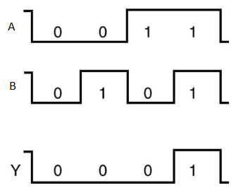
Timing Diagram:
OR gate
It is a digital circuit which has two or more inputs and a single output which is the logical OR of all those inputs. It is represented with the symbol ‘+’.
The truth table of 2-input OR gate is:
A | B | Y = A + B |
0 | 0 | 0 |
0 | 1 | 1 |
1 | 0 | 1 |
1 | 1 | 1 |
Here A, B are the inputs and Y is the output of two input OR gate.
When both inputs are ‘0’, then only the output, Y is ‘0’. For remaining combinations of inputs, the output, Y is ‘1’.
The figure below shows the symbol of an OR gate, which is having two inputs A, B and one output, Y.

Fig. : OR gate (ref. 1)
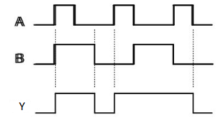
Timing Diagram:
NOT gate
It is a digital circuit that has one input and one output. Here the output is the logical inversion of input. Hence, it is also called as an inverter.
The truth table of NOT gate is:
A | Y = A’ |
0 | 1 |
1 | 0 |
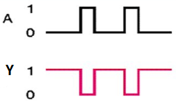
Here A and Y are the corresponding input and output of NOT gate. When A is ‘0’, then, Y is ‘1’. Similarly, when, A is ‘1’, then, Y is ‘0’.
The figure below shows the symbol of NOT gate, which has one input, A and one output, Y.
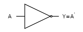
Fig. : NOT gate (ref. 1)
Timing Diagram:
Universal gates
NAND & NOR gates are known as universal gates.
We can implement any Boolean function by using NAND gates and NOR gates alone.
NAND gate
It is a digital circuit which has two or more inputs and single output and it is the inversion of logical AND gate.
The truth table of 2-input NAND gate is:
A | B | Y = (A.B)’ |
0 | 0 | 1 |
0 | 1 | 1 |
1 | 0 | 1 |
1 | 1 | 0 |
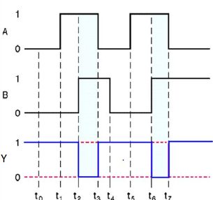
Here A, B are the inputs and Y is the output of two input NAND gate. When both inputs are ‘1’, then the output, Y is ‘0’. If at least one of the input is zero, then the output, Y is ‘1’. This is just the inverse of AND operation.
The image shows the symbol of NAND gate:

Fig.: NAND gate (ref. 1)
NAND gate works same as AND gate followed by an inverter.
Timing Diagram:
NOR gate
It is a digital circuit that has two or more inputs and a single output which is the inversion of logical OR of all inputs.
The truth table of 2-input NOR gate is:
A | B | Y = (A+B)’ |
0 | 0 | 1 |
0 | 1 | 0 |
1 | 0 | 0 |
1 | 1 | 0 |
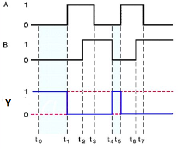
Here A and B are the two inputs and Y is the output. If both inputs are ‘0’, then the output is ‘1’. If any one of the input is ‘1’, then the output is ‘0’. This is exactly opposite to two input OR gate operation.
The symbol of NOR gate is:

Fig.: NOR gate (ref. 1)
NOR gate works exactly same as that of OR gate followed by an inverter.
Timing Diagram:
Special Gates
Ex-OR gate
It stands for Exclusive-OR gate. Its function varies when the inputs have even number of ones.
The truth table of 2-input Ex-OR gate is:
A | B | Y = A⊕B |
0 | 0 | 0 |
0 | 1 | 1 |
1 | 0 | 1 |
1 | 1 | 0 |
Here A, B are the inputs and Y is the output of two input Ex-OR gate. The output (Y) is zero instead of one when both the inputs are one.
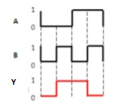
Therefore, the output of Ex-OR gate is ‘1’, when only one of the two inputs is ‘1’. And it is zero, when both inputs are same.
The symbol of Ex-OR gate is as follows:
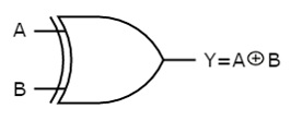
Fig.: XOR gate (ref. 1)
It is similar to that of OR gate with an exception for few combination(s) of inputs. Hence, the output is also known as an odd function.
Timing Diagram:
Ex-NOR gate
It stands for Exclusive-NOR gate. Its function is same as that of NOR gate except when the inputs having even number of ones.
The truth table of 2-input Ex-NOR gate is:
A | B | Y = A⊙B |
0 | 0 | 1 |
0 | 1 | 0 |
1 | 0 | 0 |
1 | 1 | 1 |
Here A, B are the inputs and Y is the output. It is same as Ex-NOR gate with the only modification in the fourth row. The output is 1 instead of 0, when both the inputs are one.
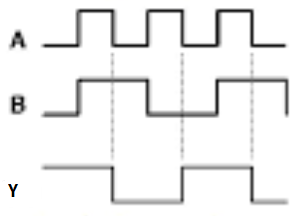
Hence the output of Ex-NOR gate is ‘1’, when both inputs are same and 0, when both the inputs are different.
The symbol of Ex-NOR gate is:
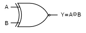
Fig.: XNOR gate (ref. 1)
It is similar to NOR gate except for few combination(s) of inputs. Here the output is ‘1’, when even number of 1 is present at the inputs. Hence is also called as an even function.
Timing Diagram:
- It is a combinational circuit which has two inputs and two outputs.
- It is designed to add two single bit binary number A and B.
- It has two outputs carry and sum.
Block diagram
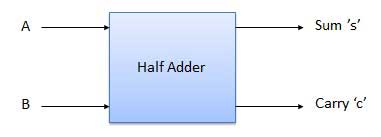
Fig. : Half adder (ref. 2)
Truth Table
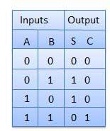
Circuit Diagram
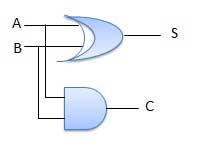
Fig.: Half adder (ref. 2)
- It is developed to overcome the drawback of Half Adder circuit.
- It can add two one-bit numbers A and B and a carry C.
- It is a three input and two output combinational circuit.
Block diagram
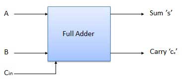
Fig. : Full adder (ref. 2)
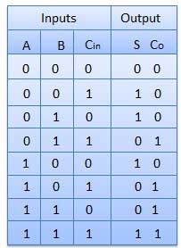
Circuit Diagram
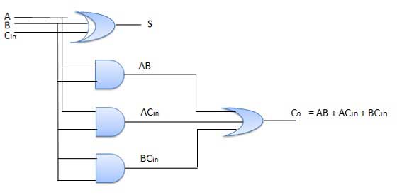
Fig. : Full adder (ref. 2)
Multiplexer is a combinational circuit that has maximum of 2n data inputs, ‘n’ selection lines and single output line. One of these data inputs will be connected to the output based on the values of selection lines.
Since there are ‘n’ selection lines, there will be 2n possible combinations of zeros and ones. So, each combination will select only one data input. Multiplexer is also called as Mux.
4x1 Multiplexer
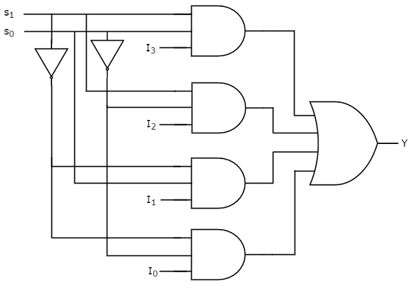
4x1 Multiplexer has four data inputs I3, I2, I1 & I0, two selection lines s1 & s0 and one output Y. The block diagram of 4x1 Multiplexer is shown in the following figure.
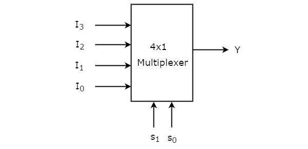
One of these 4 inputs will be connected to the output based on the combination of inputs present at these two selection lines. Truth table of 4x1 Multiplexer is shown below.
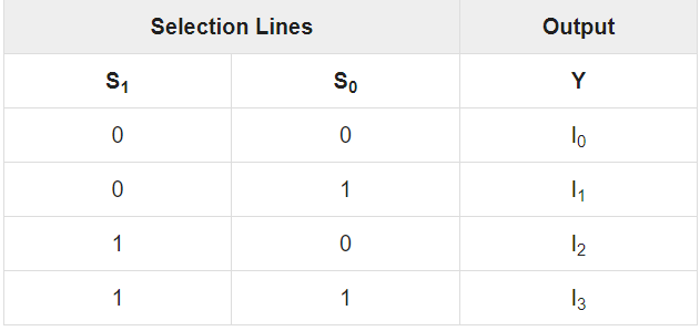
From Truth table, we can directly write the Boolean function for output, Y as
Y=S1′S0′I0+S1′S0I1+S1S0′I2+S1S0I3
We can implement this Boolean function using Inverters, AND gates & OR gate. The circuit diagram of 4x1 multiplexer is shown in the following figure.
A decoder is a circuit that changes a code into a set of signals. It is called a decoder because it does the reverse of encoding.
Types of Decoders
Line Decoder
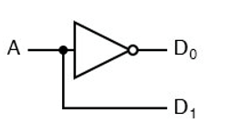
A common type of decoder is the line decoder which takes an n-digit binary number and decodes it into 2n data lines. The simplest is the 1-to-2 line decoder. The truth table is:
A D1 D0
0 0 1
1 1 0
A is the address and D is the data line. D0 is NOT A and D1 is A.
The circuit looks like the Figures below.
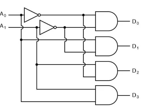
2 to 4 Line Decoder
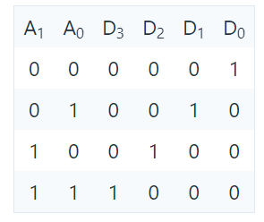
The truth table is
Larger line decoder:
Larger line decoders can be designed in a similar fashion, but just like with the binary adder there is a way to make larger decoders by combining smaller decoders. An alternate circuit for the 2-to-4 line decoder is:
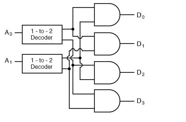
Replacing the 1-to-2 Decoders with their circuits will show that both circuits are equivalent. In a similar fashion a 3-to-8 line decoder can be made from a 1-to-2 line decoder and a 2-to-4 line decoder, and a 4-to-16 line decoder can be made from two 2-to-4 line decoders.
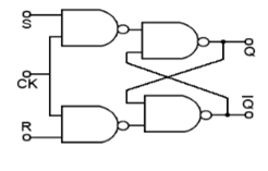
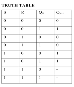
SR Flip Flop
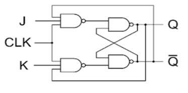
JK Flip Flop
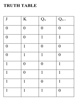
Race Around Condition In JK Flip-flop –
- For J-K flip-flop, if J=K=1, and if clk=1 for a long period of time, then output Q will toggle as long as CLK remains high which makes the output unstable or uncertain.
- This problem is known as race around condition in J-K flip-flop.
- This problem can be avoided by ensuring that the clock input is at logic “1” only for a very short time.
- Hence the concept of Master Slave JK flip flop was introduced.
Master Slave JK flip flop –
It is basically a combination of two JK flip-flops connected together in series.
The first is the “master” and the other is a “slave”.
The output from the master is connected to the two inputs of the slave whose output is fed back to inputs of the master.
In addition to these two flip-flops, the circuit comprises of an inverter.
The inverter is connected to clock pulse in such a way that an inverted clock pulse is given to the slave flip-flop.
In other words if CP=0 for a master flip-flop, then CP=1 for a slave flip-flop and vice versa.
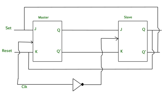
Fig. Master Slave Flip flop
Working of a master slave flip flop –
- When the clock pulse goes high, the slave is isolated; J and K inputs can affect the state of the system. The slave flip-flop is isolated when the CP goes low. When the CP goes back to 0, information is transmitted from the master flip-flop to the slave flip-flop and output is obtained.
- The master flip flop is positive level triggered and the slave flip flop is negative level triggered, hence the master responds prior to the slave.
- If J=0 and K=1, Q’ = 1 then the master goes to the K input of the slave and the clock forces the slave to reset therefore the slave copies the master.
- If J=1 and K=0, Q = 1 then the master goes to the J input of the slave and the Negative transition of the clock sets the slave and thus copy the master.
- If J=1 and K=1, the master toggles on the positive transition and the slave toggles on the negative transition of the clock.
- If J=0 and K=0, the flip flop becomes disabled and Q remains unchanged.
Timing Diagram of a Master flip flop –
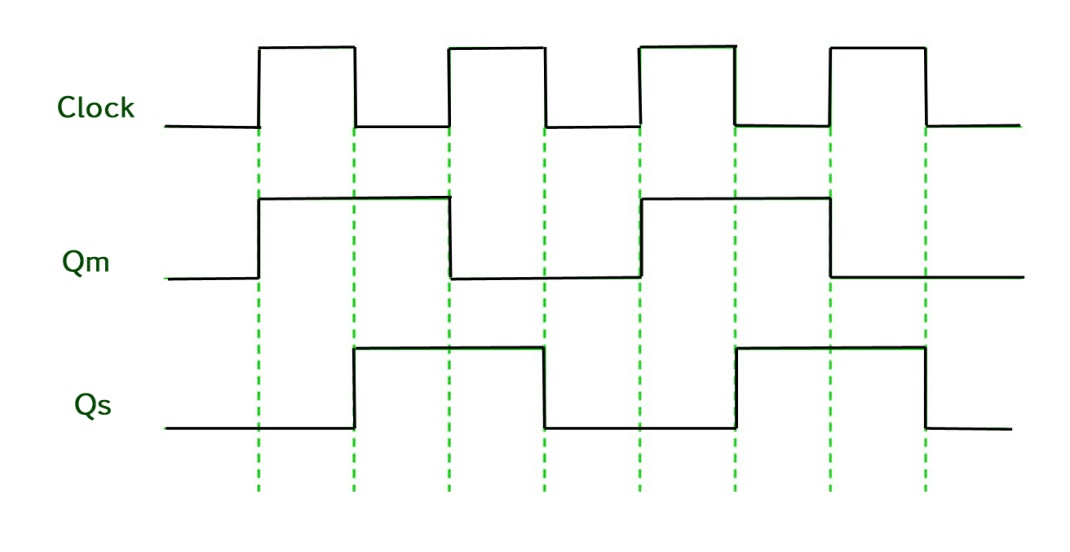
- When the CP = 1 then the output of master is high and remains high till CP = 0 because the state is stored.
- Now the output of master becomes low when the clock CP = 1 and remains low until the clock becomes high again.
- Thus toggling takes place for a clock cycle.
- When the CP = 1 then the master is operational but not the slave.
- When the clock is low, the slave becomes operational and remains high until the clock again becomes low.
- Toggling takes place during the whole process since the output changes once in a cycle.
- This makes the Master-Slave J-K flip flop a Synchronous device which passes data with the clock signal.
Shift Registers are used for data storage or for the movement of data and are therefore commonly used inside calculators or computers to store data such as two binary numbers before they are added together, or to convert the data from either a serial to parallel or parallel to serial format.
The individual data latches that make up a single shift register are all driven by a common clock ( Clk ) signal making them synchronous devices.
Shift register IC’s are generally provided with a clear or reset connection so that they can be “SET” or “RESET” as required. Generally, shift registers operate in one of four different modes with the basic movement of data through a shift register being:
- Serial-in to Parallel-out (SIPO) - the register is loaded with serial data, one bit at a time, with the stored data being available at the output in parallel form.
- Serial-in to Serial-out (SISO) - the data is shifted serially “IN” and “OUT” of the register, one bit at a time in either a left or right direction under clock control.
- Parallel-in to Serial-out (PISO) - the parallel data is loaded into the register simultaneously and is shifted out of the register serially one bit at a time under clock control.
- Parallel-in to Parallel-out (PIPO) - the parallel data is loaded simultaneously into the register, and transferred together to their respective outputs by the same clock pulse.
A n-bit ripple counter can count up to 2n states. It is also known as MOD n counter. It is known as ripple counter because of the way the clock pulse ripples its way through the flip-flops. Some of the features of ripple counter are:
- It is an asynchronous counter.
- Different flip-flops are used with a different clock pulse.
- All the flip-flops are used in toggle mode.
- Only one flip-flop is applied with an external clock pulse and another flip-flop clock is obtained from the output of the previous flip-flop.
- The flip-flop applied with external clock pulse act as LSB (Least Significant Bit) in the counting sequence.
A counter may be an up counter that counts upwards or can be a down counter that counts downwards or can do both i.e.count up as well as count downwards depending on the input control.
The sequence of counting usually gets repeated after a limit. When counting up, for n-bit counter the count sequence goes from 000, 001, 010, … 110, 111, 000, 001, … etc. When counting down the count sequence goes in the opposite manner: 111, 110, … 010, 001, 000, 111, 110, … etc.
3-bit Ripple counter using JK flip-flop –
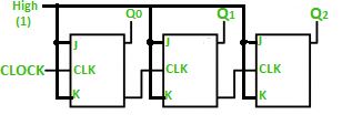
In the circuit shown in above figure, Q0(LSB) will toggle for every clock pulse because JK flip-flop works in toggle mode when both J and K are applied 1, 1 or high input. The following counter will toggle when the previous one changes from 1 to 0.
Truth Table –
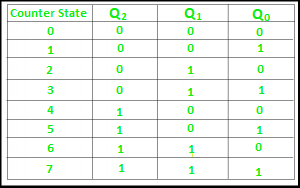
The 3-bit ripple counter used in the circuit above has eight different states, each one of which represents a count value. Similarly, a counter having n flip-flops can have a maximum of 2 to the power n states. The number of states that a counter owns is known as its mod (modulo) number. Hence a 3-bit counter is a mod-8 counter.
A mod-n counter may also be described as a divide-by-n counter. This is because the most significant flip-flop (the furthest flip-flop from the original clock pulse) produces one pulse for every n pulses at the clock input of the least significant flip-flop (the one triggers by the clock pulse). Thus, the above counter is an example of a divide-by-4 counter.
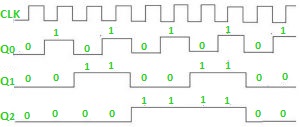
Timing diagram – Let us assume that the clock is negative edge triggered so above counter will act as an up counter because the clock is negative edge triggered and output is taken from Q.

The necessary components of communication system are information source , input transducer, transmitter, communication channel, receiver and destination.
The function of the blocks:
Information Source:
A communication system serves to communicate a message or information or data. This information/data originates in the information source.
There can be different messages in the form of words, group of words, code symbols, sound signals etc. However, out of these messages only the desired messages is chosen and communicated.
Therefore, the information source produces the required messages which has to be transmitted.
Input transducer:
The input can be in any energy form but for transmission purpose it needs to be converted to electrical energy. The transducer does this :
An electronic communication system that come across devices that either their inputs or outputs in electrical form.
Any device that converts one form of energy/power into another is termed as transducer.
An electrical transducer defined as an apparatus that converts physical changeable (pressure, force, or temperature etc into variations within the electrical signal at its output.
Transmitter:
It converts information/data into a signal that is suitable for transmission over a medium. Transmitters increases the power of the signal thro power amplifiers and also provides interfaces to match the transmission medium such as antenna interface, fiber interface and so on. The operate of the transmitter is to process the electrical signal from different aspects.
Channel:
- The channel refers to the medium through which an electrical signal travels. These media are classified into two types such as guided and unguided.
- Guided media is directed from source in the direction of the receiver by using connective cables. In OFC-optical fiber communication an optical fiber is a medium.
- The unguided media refers to the communication channel that forms space amng the source as well as the receiver. In RF(radio frequency) communication, the medium space is called air. It is the only thing among the source and receiver but in sonar the medium is generally water since sound waves tour powerfully through assured liquid media.
- The two types of media are measured unguided for the reason that there are no connecting wrires between the source as well as the receiver.
Noise :
It is the undesirable electric energy that enters the communication system and interferes with the desired signal.
A cellular/mobile system provides standard telephone operation by full-duplex two-way radio at remote locations. It provides a wireless connection to the Public Switched Telephone Network (PSTN) from any user location within the radio range of the system.
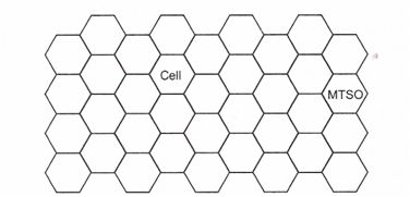
The basic concept behind the cellular radio system is that rather than serving a given geographical area within a single transmitter and receiver, the system divides the service area into many small areas known as cells, as shown in Fig. Below.
The typical cell covers only several square kilometers and contains its own receiver and low-power transmitter. The cell area shown in Fig. Below is ideal hexagon. However, in reality they will have circular or other geometric shapes. These areas may overlap, and cells may be of different sizes.
Basic cellular system consists of mobile stations, base stations and a mobile switching center (MSC). The MSC is also known as Mobile Telephone Switching Office (MTSO). The MTSO controls ’11 the cells and provides the interface between each cell and the main telephone office. Each mobile communicates via radio with one of the base stations and may be handed off (switched from one cell to another) to any other base station throughout the duration of the call.
Each mobile station consists of a transceiver, an antenna and control circuitry. The base station consists of several transmitters and receivers which simultaneously handle full duplex communication and generally have towers which support several transmitting and receiving antennas.
The base station serves as a bridge between all mobile users in the cell and connects the simultaneous mobile calls via telephone lines or microwave link to the MSC. The MSC co-ordinates the activities of all the base stations and connects the entire cellular system to the PSTN, most of the cellular system also provide a service known as roaming.
The cellular system operates in the 800-900 MHz range. The newer digital cellular systems have even greater capacity. Some of these systems operate in 1.7-1.8 GHz bands.
CELLULAR TELEPHONE UNIT
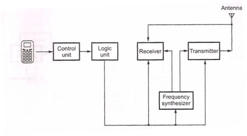
The Fig. Below shows the block diagram of a cellular mobile radio unit. The unit consists of five major sections:
Transmitter, receiver, synthesizer, logic unit, and control unit. The mobile unit contains built-in rechargeable batteries to Provide operating power. The transmitter and receiver in the unit share the common antenna.
References:
ELECTRONIC DEVICES AND CIRCUITS by VENKATA RAO, McGraw Hill
Getting started in Electronics by Forrest.M.Mims
All New Electronics – Self Teaching Guide by Harry Kybett & Earl Boysen
Practical Electronics for Inventors by Paul Scherz