UNIT 5
MATERIAL SCIENCE
The classical free electron theory of metals (Drude –Lorentz theory of metals) Drude and Lorentz proposed this theory in 1900. According to this theory, the metals containing the free electrons obey the laws of classical mechanics.
Assumptions (or salient features) in classical free electron theory
The classical free electron theory is based on the following postulates.
1. The valence electrons of atoms are free to move about the whole volume of the metal, like the molecules of a perfect gas in a container.
2. The free electrons move in random direction and collide with either positive ions fixed to the lattice or the other free electrons. All the collisions are elastic in nature i.e., there is no loss of energy.
3. The momentum of free electrons obeys the laws of the classical kinetic theory of gases.
4. The electron velocities in a metal obey classical Maxwell-Boltzman distribution of velocities.
5. When the electric field is applied to the metal, the free electrons are accelerated in the direction opposite to the direction of applied electric field.
6. The mutual repulsion among the electrons is ignored, so that they move in all the directions with all possible velocities.
7. In the absence of the field, the energy associated with an electron at temperature T is given by  kT. It is related to the kinetic energy equation
 kT =
kT = v2th
v2th
Here vth represents the thermal velocity.
Success of classical free electron theory
1. It verifies ohm’s law
2. It explains electrical conductivity of metals.
3. It explains thermal conductivity of metals.
4. It derives Widemann – Franz law. (i.e. the relation between electrical and thermal conductivity.
Draw backs of classical free electron theory.
1. It could not explain the photoelectric effect, Compton Effect and black body radiation.
2. Electrical conductivity of semiconductors and insulators could not be explained.
3. Widemann – Franz law (K/σT= constant) is not applicable at lower temperatures.
4. Ferromagnetism could not be explained by this theory. The theoretical value of paramagnetic susceptibility is greater than the experimental value.
5. According to classical free electron theory the specific heat of metals is given by 4.5R whereas the experimental value is given by 3R.
6. According to classical free electron the electronic specific heat is equal to 3/2R while the actual value is 0.01R.
Electrical Conductivity
The classical free electron theory was proposed by Drude and Lorentz. According to this theory the electrons are moving freely and randomly moving in the entire volume of the metal like gas atoms in the gas container. When an electric field is applied the free electrons gets accelerated.
When an electric field E is applied between the two ends of a metal of area of cross section A
When an electrical field (E) is applied to an electron of charge ‘e’ of a metallic rod, the electron moves in opposite direction to the applied field with a velocity vd. This velocity is known as drift velocity.
Drift velocity vd is defined as the average velocity of the free electrons with which they move towards the positive terminal under the influence of the electrical field.
Lorentz force acting on the electron F = eE ........(1)
This force is known as the driving force of the electron.
Due to this force, the electron gains acceleration ‘a’.
From Newton’s second law of motion,
Force F = ma …....(2)
From the equation (1) and (2),
ma = eE or
a =  …......(3)
Acceleration (a) = 
Or a =
Relaxation time is defined as the time taken by a free electron to reach its equilibrium position from the disturbed position in the presence of an electric field.
So vd = a ……….(4)
Substituting equation (3) in (4)
vd =  =
=  E ……….(5)
vd =  E ……….(5a)
Where  = RMS velocity
The Ohms’ law states that current density (J) is expressed as
J =E ……….(6)
Or = 
Where is the electrical conductivity of the electron.
But, the current density in terms of drift velocity is given as
J = nevd ....... (7)
Substituting equation (5) in equation (7), we have
J = ne E
E
Or  =
= 
On comparing the equation (6) and (8) , we have
Electrical conductivity
=  ....... (8)
=  ....... (8a)
This is a required expression for electrical conductivity.
Resistivity ρ
ρ =  =
= 
According to kinetic theory of gasses
 =
= 
So =  =
=
Also
ρ =  =
= 
Mobility: It is defined as the drift velocity of the charge carrier per unit applied electric field.
μ=  ....... (9)
From equation (7) we have
J = nevd
by substituting vd =μEfrom equation (9)
J = neμE
Or  = μne ....... (10)
We know by ohms law =  so equation (10) can be rewritten as
= μne
μ = 
This is the required expression for mobility.
Temperature Dependence
The positive ions are always in oscillating (or vibrating) state about their mean position; even the substance is present at 0k temperature. The vibrating amplitude of ions is always depends the temperature. The mean free path λ of the electrons is inversely proportional to the mean square of amplitude of ionic vibrations A0
λ =  ………(1)
The energy of lattice vibrations is proportional to  and increases linearly with temperature T.
  T ……….(2)
From equations (1) and (2)
λ =  ………..(3)
The resistivity ρ of the metal is inversely proportional to mean free path of electrons λ
ρ =  ..…………..(4)
From equations (3) and (4)
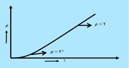
ρ T ..……….(5)
From equation (5) we observe that the resistivity of metal is linearly increases with temperature. The conductivity is defined as the reciprocal of resistance.
 ………….(6)
From equation (6) we observe that the conductivity of metal is inversely proportional to their temperature. The variation of resistivity of metal with temperature is shown in figure.
|
Figure 1:Variation of resistivity of metal with temperature
Key Takeaways
- According to this theory, the metals containing the free electrons obey the laws of classical mechanics.
- The valence electrons of atoms are free to move about the whole volume of the metal, like the molecules of a perfect gas in a container.
- The free electrons move in random direction and collide with either positive ions fixed to the lattice or the other free electrons. All the collisions are elastic in nature i.e., there is no loss of energy.
- Theory successfully explains the ohm’s law, electrical conductivity of metals and thermal conductivity of metals also give the relation between electrical and thermal conductivity.
- The required expression for electrical conductivity is given by =

- Resistivity ρ is given asρ =
 =
= 
- Mobility is defined as the drift velocity of the charge carrier per unit applied electric field and given by μ =
 .
.
The failure of classical free electron theory paved this way for Quantum free electron theory. It is introduced by Sommerfeld in 1928. Arnold Sommerfeld overcomes many drawbacks of the classical free electron theory by applying quantum mechanical principles in 1928.
Quantization of electrical energy levels is added here. He also used the Pauli Exclusion Principle in restricting the energy values of electron. His theory is known as Quantum Free Electron Theory
The main assumptions of quantum free electron theory are,
- In a metal the available free electrons are fully responsible for electrical conduction.The energy levels of the electrons that responsible for the conduction are quantised.
- The electrons move in a constant potential inside the metal but they cannot come out from this potential but remain confined within its boundaries.
- The distribution of electrons in various allowed energy levels occur according to the Pauli Exclusion Principle.
- Electrons have wave nature, the velocity and energy distribution for the electrons given by Fermi-Dirac distribution function.
- Both the attraction between the electrons and the lattice ions, and the repulsion between the electrons themselves are ignored.
- The energy is loss due to interaction of the free electron with the other free electron
Key Takeaways
- The failure of classical free electron theory paved this way for Quantum free electron theory. It is introduced by Sommerfeld in 1928.
- Arnold Sommerfeldovercomes many drawbacks of the classical free electron theory by applying quantum mechanical principles in 1928.
- Quantization of electrical energy levels is added here.
- He also used the Pauli Exclusion Principle in restricting the energy values of electron.
A parameter of interest in the study of conductivity of metals and semiconductors is the density of states.
Density of Energy States
The Fermi function gives the probability of occupying an available energy state, but this must be factored by the number of available energy states to determine how many electrons would reach the conduction band. This density of states is the electron density of states, but there are differences in its implications for conductors and semiconductors. For the conductor, the density of states can be considered to start at the bottom of the valence band and fill up to the Fermi level, but since the conduction band and valence band overlap, the Fermi level is in the conduction band so there are plenty of electrons available for conduction. In the case of the semiconductor, the density of states is of the same form, but the density of states for conduction electrons begins at the top of the gap.
The Fermi function F(E) gives only the probability of filling up of electrons in a given energy state. It does not give the information about the number of electrons that can be filled in a given energy state, to know that we should know the number of available energy states called density of states.
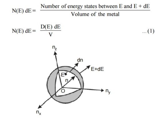
Density of states is defined the as the number of energy states per unit volume in an energy interval of a metal. It is used to calculate the number of charge carriers per unit volume of any solid.
|
Figure 2: Positive octant of n space
Let us constant a sphere of radius “n” in space with quantum numbers nn, ny and nz
|
The sphere is further divided into many shells represents a particular combination of quantum numbers and represents particular energy value.
Therefore, the number of energy states within a sphere of radius
|
Let us consider two energy values E and E + dE can be found by finding the number of energy states between the shells of radius n and n+ dn from the origin. Since the quantum numbers are positive integers, n values can be defined only in the positive octant of the n – space.
The number of available energy states within the sphere of radius “n” due to one octant.
|
Similarly the number of available energy states within the sphere of radius n+dn corresponding energy.
|
The number of available energy states between the shells of radius n and n + dn (or) between the energy levels E and E + dE
|
The number of available energy states between the energy interval dE
|
Since the higher powers of dn is very small, dn2 and dn3 terms can be neglected.
|
We know that the allowed energy values is
|
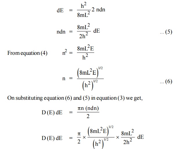
Differentiating equation (4) with respect to ‘n’
|
|
Key Takeaways
- The Fermi function gives the probability of occupying an available energy state, but this must be factored by the number of available energy states to determine how many electrons would reach the conduction band.
- This density of states is the electron density of states, but there are differences in its implications for conductors and semiconductors.
- Density of states is defined the as the number of energy states per unit volume in an energy interval of a metal. It is used to calculate the number of charge carriers per unit volume of any solid.
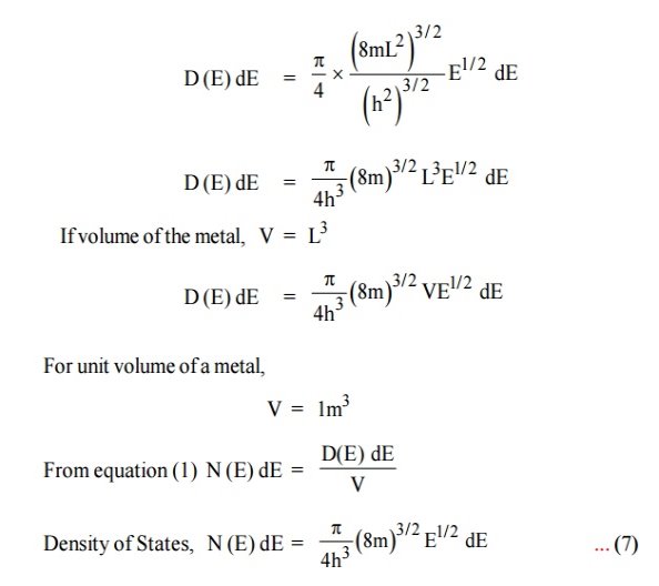
- Density of state is given by
|
The Fermi function gives the probability of occupying an available energy state, but this must be factored by the number of available energy states to determine how many electrons would reach the conduction band.
When the temperature is not at absolute zero, the material will be receiving thermal energy from surroundings. However at ordinary temperature, the amount of energy an electron can gain is quite small, because of which the electrons occupying energy levels below the Fermi level.
However, there are unoccupied higher energy levels which are above the occupied energy levels at small energy differences. They are located near Fermi level. Those are the energy levels into which, the electrons in the energy levels near Fermi level, are capable of being excited.
During thermal excitation when the temperature is greater than 0K (i.e., T >0), the electrons which absorb the thermal energy move into higher energy levels which were unoccupied at zero degree absolute (i.e., T = 0).
Such excitations seem to be random, the occupation of various energy level obey a statistical distribution called Fermi-Dirac distribution.
Fermi function F (E):
Fermi-Dirac distribution function represents the probability of an electron occupying a given energy level at absolute temperature. It is given by Fermi factor F(E) or f(E).

Where KB Boltzmann Constant
T Temperature
Ifg(E) is the density of states andf(E) gives the probability of occupationof those states at a given temperature, the number of occupied states,n(E),is given by
n(E) = (1)
(1)
If the number of occupied states in an energy band needs to be calculatedthe integration needs to be performed over the entire band. This will be afunction of temperature, since the Fermi function is temperature dependent.Equation 1 can be used to calculate the concentration of electron and holesin semiconductors, which decides their conductivity.
Effect of temperature on Fermi Function:
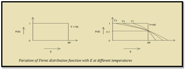
Case (i) Probability of occupation for E < EF at T = 0K

When T = 0K and E < EF, we have
F(E) =  =
=  = 1
= 1
Thus at T = 0K, there is 100 % chance for the electrons to occupy the energy levels below the Fermi level.
|
Figure 3: Fermi distribution
Case (ii) Probability of occupation for E>EF at T = 0K
When T = 0K and E > EF, we have
F(E) =  =
=  =
=  = 0
= 0
Thus, there is 0 % chance for the electrons to occupy energy levels above the Fermi energy level. From the above two cases, at T = 0K the variation of F(E) for different energy values becomes a stepfunction.
Case (iii) Probability of occupation at ordinary temperature
At ordinary temperature, the value of probability starts reducing from 1 for values of E slightly less than EF. With the increase of temperature, i.e., T> 0K, Fermi function F (E) varies with E.
At any temperature other than 0K and E = EF
F(E) =  =
=  =
=  = 50%
= 50%
Hence, there is 50 % chance for the electrons to occupy Fermi level. Further, for E > EF the probability value falls off rapidly to zero.
Case (iv) At high temperature
When kT >> EF, the electrons lose their quantum mechanical character and Fermi distribution function reduces to classical Boltzmann distribution
Key Takeaways
- The Fermi function gives the probability of occupying an available energy state,
- Fermi-Dirac distribution function represents the probability of an electron occupying a given energy level at absolute temperature. It is given by Fermi factor F(E) or f(E).

- Thus at T = 0K, there is 100 % chance for the electrons to occupy the energy levels below the Fermi level.
- At any temperature other than 0K and E = EF, there is 50 % chance for the electrons to occupy Fermi level.
- At high temperature , the electrons lose their quantum mechanical character and Fermi distribution function reduces to classical Boltzmann distribution
FERMI LEVEL
Fermi level" is the term used to describe the top of the collection of electron energy levels at absolute zero temperature. This concept comes from Fermi-Dirac statistics. Electrons are fermions and by the Pauli exclusion principle cannot exist in identical energy states. So at absolute zero they pack into the lowest available energy states and build up a "Fermi sea" of electron energy states. The Fermi level is the surface of that sea at absolute zero where no electrons will have enough energy to rise above the surface.
The concept of the Fermi energy is a crucially important concept for the understanding of the electrical and thermal properties of solids. Both ordinary electrical and thermal processes involve energies of a small fraction of an electron volt. But the Fermi energies of metals are on the order of electron volts. This implies that the vast majority of the electrons cannot receive energy from those processes because there are no available energy states for them to go to within a fraction of an electron volt of their present energy. Limited to a tiny depth of energy, these interactions are limited to "ripples on the Fermi sea".
At higher temperatures a certain fraction, characterized by the Fermi function, will exist above the Fermi level. The Fermi level plays an important role in the band theory of solids. In doped semiconductors, p-type and n-type, the Fermi level is shifted by the impurities, illustrated by their band gaps. The Fermi level is referred to as the electron chemical potential in other contexts.
The Fermi energy also plays an important role in understanding the mystery of why electrons do not contribute significantly to the specific heat of solids at ordinary temperatures, while they are dominant contributors to thermal conductivity and electrical conductivity. Since only a tiny fraction of the electrons in a metal are within the thermal energy kT of the Fermi energy, they are "frozen out" of the heat capacity by the Pauli principle. At very low temperatures, the electron specific heat becomes significant.
It is named after the Physicist Enrico Fermi. A Fermi level is the measure of the energy of least tightly held electrons within a solid. It is important in determining the thermal and electrical properties of solids. It can be defined as:
The Fermi energy is a concept in quantum mechanics usually refers to the energy difference between the highest and lowest occupied single-particle states in a quantum system of non-interacting fermions at absolute zero temperature.
The value of the Fermi level at absolute zero temperature is known as the Fermi energy. It is also the maximum kinetic energy an electron can attain at 0K. Fermi energy is constant for each solid.
To determine the lowest possible Fermi energy of a system, we first group the states with equal energy into sets and arrange them in increasing order of energy. We then add particles one at a time, successively filling up the unoccupied quantum states with the lowest energy.
When all the particles are arranged accordingly, the energy of the highest occupied state is the Fermi energy.
In Spite of the extraction of all possible energy from metal by cooling it to near absolute zero temperature (0 Kelvin), the electrons in the metal still move around. The fastest ones move at a velocity corresponding to a kinetic energy equal to the Fermi energy.
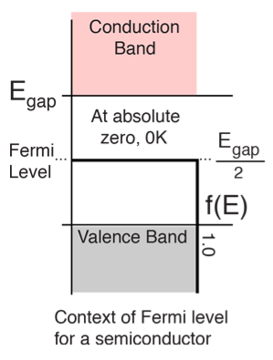
The highest energy level that an electron can occupy at the absolute zero temperature is known as the Fermi Level. The Fermi level lies between the valence band and conduction band because at absolute zero temperature the electrons are all in the lowest energy state. Due to lack of sufficient energy at 0 Kelvin, the Fermi level can be considered as the sea of fermions (or electrons) above which no electrons exist. The Fermi level changes as the solids are warmed and as electrons are added to or withdrawn from the solid.
Don’t get confuse between Fermi level and Fermi energy.Both the terms are equal at absolute zero temperature but they are different at other temperature.
Derivation of the expression for Fermi energy
Let us recall the formula for density of states (we derived density of states under article 5.4, equation 7)
|
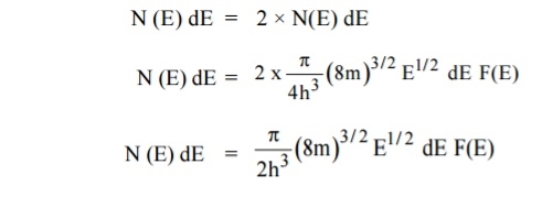
Each electron energy level can accommodate two electrons as per Pauli’s exclusion principle. (Spin up and Spin down = 2 (e) × density of states).
|
Carrier Concentration In Metals
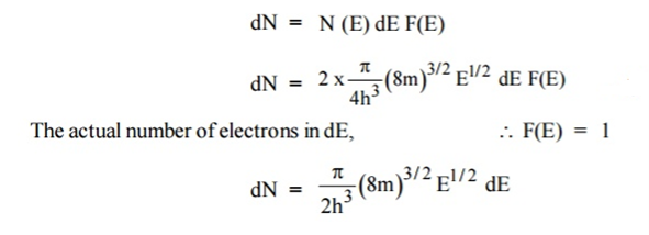
Let N(E) dE represents the number of filled energy states between the interval of energy dE, normally all the energy states will not be filled
dN = N (E) dE F(E)
|
Normally all the states are not filled states, filling of electrons is a given energy state is given by Fermi-function F(E). Let dn represents the number of filled energy states.
In this case of material of absolute zero the upper occupied level is EF and for all the levels below EF, F(E)=1 (at T = 0 K the maximum energy level that can be occupied by the electron is called Fermi energy level EF T = 0 K F(E) = 1).
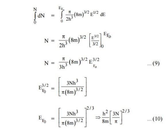
Integrating equation (8) within the limits 0 to EF0 us can get the number of energy states of electron (N)
|
Hence the Fermi energy of a metal depends only on the density of electrons of that metal.
In metals, the Fermi energy gives us information about the velocities of the electrons which participate in ordinary electrical conduction. The amount of energy which can be given to an electron in such conduction processes is on the order of micro-electron volts (see copper wire example), so only those electrons very close to the Fermi energy can participate. The Fermi velocity of these conduction electrons can be calculated from the Fermi energy.
This speed is a part of the microscopic Ohm's Law for electrical conduction. For a metal, the density of conduction electrons can be implied from the Fermi energy. |
Figure 4: Fermi level for a Semiconductor
| |||
|
|
Success of QFET
1. This theory explains the specific heat capacity of materials.
One of thedifficultiesis to the heat capacity of the conductionelectrons. According to classical theory a free particle should have a heat capacity of where
where , is the Boltzmann constant.
If we have N number of atomsand each give one valence electron to the electron gas, and the electrons are freely mobile, then the electronic contribution to the heat capacity should be , same as for the case of atoms of a monatomic gas. But the observed electronic contributionat room temperature is usually less than this value.
How can the electrons participate in electrical conduction processes as if they were mobile, while not contributing to the heat capacity?
This important discrepancy is removed with the help of Quantum theory of free electrons. It was discovered that the specific heat vanishes at absolute zero and that at lowtemperatures it is proportional to the absolute temperature.
When we heat the specimen from absolute zero, not every electron gains energy as expected classically, but only those electrons in orbitals within an energy range
 of the Fermi level are excited thermally. This gives an immediate qualitative solution to the problem of the heat capacity of the conduction electron gas.
If N is the total number of electrons, only a fraction of the order of T/TF can he excited thermally at temperature T,
This is because only these electrons lie within an energy range of the order of  of the top of the energy distribution.
Each of these NT/TF electrons has a thermal energy of the order of kBT.
The total electronic thermal kinetic energy U is of the order of
U  (NT/TF)
The electronic heat capacity is given by
C = 
and is directly proportional to T, in agreement with the experimentalresults discussed in the following section. At room temperature C is smallerthan the classical value , by a factor of the order of 0.01 or less, forTF
 5
5  104K.
104K.
2. This theory explains photo electric effect, Compton Effect and block body radiation etc.
3. This theory gives the correct mathematical expression for the thermalconductivity of metals
The temperature-dependent part of the electrical resistivity is proportionalto the rate at which an electron collides with thermal phonons and thermal electrons. The collision rate with phonons is proportional to the concentration of thermal phonons. Here the phonon concentration is proportional to the temperature T. So using quantum theory result the thermal conductivity can be calculated.
Disadvantages of Quantum free electron theory
1. This theory fails to explain bands presence and also not able to distinguish between metal, semiconductor and Insulator
2. According to this theory, only two electrons are present in the Fermi level and they are responsible for conduction which is not true.
3. Quantum free electron theory not able to explain the positive value of Hall Co-efficient.
Key Takeaways
- The highest energy level that an electron can occupy at the absolute zero temperature is known as the Fermi Level.
- The Fermi energy is a concept in quantum mechanics usually refers to the energy difference between the highest and lowest occupied single-particle states in a quantum system of non-interacting fermions at absolute zero temperature.
- Fermi energy of a metal depends only on the density of electrons of that metal. It is given by
|
- The Fermi velocity of these conduction electrons can be calculated from the Fermi energy by using the following relation

- This theory explains the specific heat capacity of materials. photo electric effect, Compton Effect and block body radiation etc.
- This theory also gives the correct mathematical expression for the thermal conductivity of metals
PHYSICS OF SEMICONDUCTOR
Before discussing Fermi Level in intrinsic Semiconductor, let us take a quick look on semiconductor.
Semiconductors
Semiconductors are materials that have conductivity between conductors and insulators.
Semiconductors can be pure elements, such as silicon or germanium, or compounds such as gallium arsenide or cadmium selenide.
They are not good conductors nor good insulators as their name “semi”-conductors.
These materials such as silicon (Si), germanium (Ge), and gallium arsenide (GaAs), have electrical properties somewhere in the middle, between those of a “conductor” and an “insulator”.
They have very few “free electrons” because their atoms are closely grouped in a crystalline pattern called a “crystal lattice” but electrons are still able to flow, but only under special conditions.
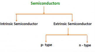
There are two basic groups or classifications that can be used to define the different semiconductor types:
- Intrinsic Semiconductor
- Extrinsic Semiconductor
|
Figure 5: Type of semiconductor
The semiconductor is divided into two types. One is an Intrinsic Semiconductor and the other is an Extrinsic semiconductor. The pure form of the semiconductor is known as the intrinsic semiconductor and the semiconductor in which intentional impurities are added for making it conductive is known as the extrinsic semiconductor.
The conductivity of the intrinsic semiconductor becomes zero at room temperature while the extrinsic semiconductor is very little conductive at room temperature. The detailed explanation of the two types of the semiconductor is given below.
INTRINSIC SEMICONDUCTOR
An intrinsic type of semiconductor material made to be very pure chemically. As a result, it possesses a very low conductivity level having very few charge carriers, namely holes and electrons, which it possesses in equal quantities.
|
Figure 6:Intrinsic Semiconductor
The most commonly used semiconductor basics material by far is silicon. Silicon has four valence electrons in its outermost shell which it shares with its neighbouring silicon atoms to form a full orbital of eight electrons. The structure of the bond between the two silicon atoms is such that each atom shares one electron with its neighbour making the bond very stable.
As there are very few free electrons available to move around the silicon crystal, crystals of pure silicon (or germanium) are therefore good insulators. Silicon atoms are arranged in a definite symmetrical pattern making them a crystalline solid structure. A crystal of pure silica (silicon dioxide or glass) is generally said to be an intrinsic crystal (it has no impurities) and therefore has no free electrons.
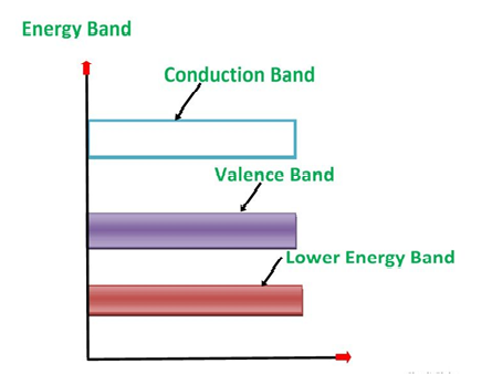
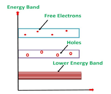
An extremely pure semiconductor is called an Intrinsic Semiconductor. Based on the energy band phenomenon, an intrinsic semiconductor at absolute zero temperature is shown below.
|
Figure 7:Intrinsic semiconductor at absolute zero temperature.
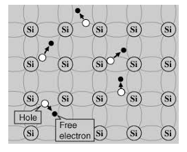
Its valence band is filled and the conduction band is empty. When the temperature is raised and some heat energy is supplied to it, some of the valence electrons are lifted to the conduction band leaving behind holes in the valence band as shown below.
|
Figure 8: Intrinsic semiconductor at T >0
A hole is the absence of an electron in a particular place in an atom. Although it is not a physical particle in the same sense as an electron, a hole can be passed from atom to atom in a semiconductor material. It is considered to have a positive charge. Holes are positive charge carriers.
The electrons reaching the conduction band move randomly. The holes created in the crystal also free to move anywhere.
This behaviour of the semiconductor shows that they have a negative temperature coefficient of resistance. This means that with the increase in temperature, the resistivity of the material decreases, and the conductivity increases.
But simply connecting a silicon crystal to a battery supply is not enough to extract an electric current from it. To do that we need to create a “positive” and a “negative” pole within the silicon allowing electrons and therefore electric current to flow out of the silicon. These poles are created by doping the silicon with certain impurities.
DOPING
The process by which an impurity is added to a semiconductor is known as Doping. The amount and type of impurity which is to be added to the material have to be closely controlled during the preparation of extrinsic semiconductor. Generally, one impurity atom is added to 108 atoms of a semiconductor.
The purpose of adding impurity in the semiconductor crystal is to increase the number of free electrons or holes to make it conductive.
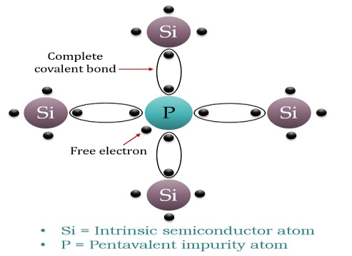
If a Pentavalent impurity, having five valence electrons is added to a pure semiconductor a large number of free electrons will exist. Which makes an n-type extrinsic semiconductor.
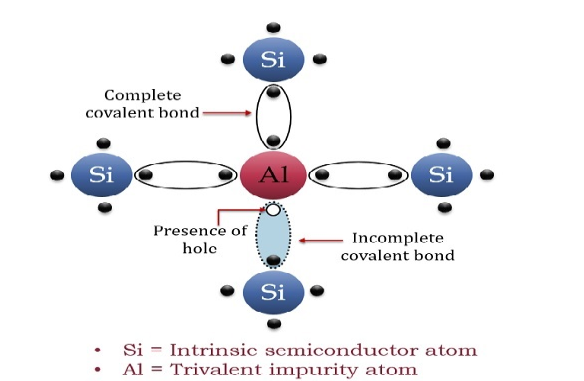
If a trivalent impurity having three valence electrons is added, a large number of holes will exist in the semiconductor. Which makes a p-type extrinsic semiconductor.
EXTRINSIC SEMICONDUCTOR
Extrinsic types of semiconductors are those where a small amount of impurity has been added to the basic intrinsic material. This 'doping' uses an element from a different periodic table group and in this way, it will either have more or fewer electrons in the valence band than the semiconductor itself. This creates either an excess or shortage of electrons. In this way two types of semiconductors are available: Electrons are negatively charged carriers. Holes are positively charged carriers.
Depending upon the type of impurity added the extrinsic semiconductor may be classified as an n-type semiconductor and p-type semiconductor.
P-TYPE EXTRINSIC SEMICONDUCTOR
The extrinsic p-Type Semiconductor is formed when a trivalent impurity is added to a pure semiconductor in a small amount, and as a result, a large number of holes are created in it. A large number of holes are provided in the semiconductor material by the addition of trivalent impurities like Gallium and Indium. Such type of impurities which produce a p-type semiconductor is known as an Acceptor Impurities because each atom of them creates one hole which can accept one electron.
In a P-type semiconductor material, there is a shortage of electrons, i.e. there are 'holes' in the crystal lattice. Electrons may move from one empty position to another and in this case, it can be considered that the holes are moving. This can happen under the influence of a potential difference and the holes can be seen to flow in one direction resulting in an electric current flow. It is harder for holes to move than for free electrons to move and therefore the mobility of holes is less than that of free electrons. Holes are positively charged carriers.
A trivalent impurity like Aluminium, having three valence electrons is added to Silicon crystal in a small amount. Each atom of the impurity fits in the Silicon crystal in such a way that its three valence electrons form covalent bonds with the three surrounding Silicon atoms as shown in the figure below.
|
Figure 9: p-Type Semiconductor
N-TYPE EXTRINSIC SEMICONDUCTOR
When a few Pentavalent impurities such as Phosphoruswhose atomic number is 15, which is categorized as 2, 8,and 5. It has five valence electrons, which are added to silicon crystals. Each atom of the impurity fits in four silicon atoms as shown in the figure below.
Hence, each Arsenic atom provides one free electron in Silicon crystal. Since an extremely small amount of Phosphorus, impurity has a large number of atoms; it provides millions of free electrons for conduction.
|
Figure 10: N-type semiconductor
An N-type semiconductor material has an excess of electrons. In this way, free electrons are available within the lattices, and their overall movement in one direction under the influence of a potential difference results in an electric current flow. This is an N-type semiconductor, the charge carriers are electrons.
Fermi Level in intrinsic Semiconductor
We know that in an intrinsic semiconductor
Electron concentration ‘n’ = Hole concentration ‘p’
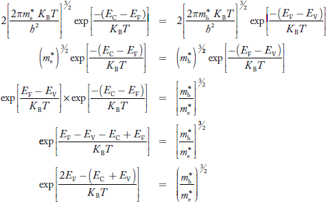
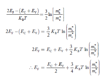
Equating Equations (15) and (27), we get
|
Taking logarithms on both sides, we get
|
……………… (29)
Normally, mh* is greater than me*, since ln  is very small so that EF is just lie inthe middle of the energy gap
Temperature effect on Fermi level
Fermi level slightly rises with an increase of temperature.
But in the case of a pure intrinsic semiconductor likeSi and Ge,
mh* ≈ me*
So in these cases,the Fermi level lies in the middle of the energy ga
Key Takeaways
- Semiconductors are materials that have conductivity between conductors and insulators.
- The semiconductor is divided into two types. One is an Intrinsic Semiconductorand the other is an Extrinsic semiconductor.
- The pure form of the semiconductor is known as the intrinsic semiconductor.
- The semiconductor in which intentional impurities are added for making it conductive is known as the extrinsic semiconductor.
- A hole is the absence of an electron in a particular place in an atom.
- The process by which an impurity is added to a semiconductor is known as Doping.
- Depending upon the type of impurity added the extrinsic semiconductor may be classified as an n-type semiconductor and p-type semiconductor.
- The extrinsic p-Type Semiconductor is formed when a trivalent impurityis added to a pure semiconductor in a small amount, and as a result, a large number of holes are created in it.
- The extrinsic n-Type Semiconductor is formed when a Pentavalentimpurityis added to a pure semiconductor in a small amount, and as a result, a large number of electrons are created in it.
- Fermi level EF is just lie inthe middle of the energy gap
- Fermi level slightly rises with an increase of temperature.
Note: only expressions are asked in your syllabus but we will discuss the whole derivation just to give you more clarity. You can remember the result only.
Intrinsic semiconductors—carrier concentration
Here we will calculate the number of electrons excited into the conduction band at temperature T and also the hole concentration in the valence band. It is assumed that the electrons in the conduction band behave as if they are free particles with effective mass me* and the holes near the top of the valence band behave as if they are free particles with effective mass mh*.
Here we will calculate the electron concentration, hole concentration
The density of Electrons in Conduction Band
The number of free electrons per unit volume of a semiconductor having energies in between E and E + dE is represented asN(E) dE
dE = width of Energy band
Therefore, we have:
N(E) dE = ge(E) dE fe(E) ……….(1)
ge(E) = The density of electron states per unit volume
fe(E)= Fermi-Dirac distribution function i.e.probability that an electron occupies an electron state
The number of electrons present in the conduction band per unit volume of material ‘n’ is obtained by integrating N(E) dE between the limits Ec and Ect
Where Ec = the bottom energy levels of the conduction band Ect = the bottom and top energy levels of the conduction band n = can be written as n = n = we know that above Ect, there are no electrons. Hence, Equation (3) becomes n = n = The Fermi-Dirac distribution function fe(E) can be represented as:
Compared to the exponential value,so the ‘1’ in the denominator can be neglected. So Hence, The density of electron states ge(E) in the energy space from E = 0 to E can be written as:
where me* is the effective mass of an electron and h is Planck’s constant.
To evaluate n, the density of states is counted from Ec, since the minimum energy state in the conduction band is Ec. so eq (8) can become
Substituting Equations (6) and (9) in (4) gives n = n = The above equation can be simplified by the following substitution: Putɛ = E − Ec ………… (11) So,dɛ = dE In Equation (11), Ec is constant, as we change the variable E to ε in Equation (10), the integral limits also change. In Equation (11),as E → Ec then ε → 0 and E →∞, then ε also →∞. the exponential term in Equation (10) becomes:
= exp [
Substituting Equations (11) and (12) in (10), we get: n = n = Above integral (I) can be simplified by substitution. Put ε = x2 so thatdɛ = 2x dx I = = = Substituting Equation (14) in (13) gives: n = n= n = n = The term n =Nc
|
The density of Holes in Valence Band
The number of holes per unit volume of semiconductor in the energy range E and E + dE in the valence band is represented as P(E) dE.Proceeding the same way(as in the case of electrons) we have
Therefore, we have:
P(E) dE = gh(E) dE fh(E) ……….(17)
dE = width ofEnergy band
gh(E) = The density of holes states per unit volume
fh(E)= Fermi-Dirac distribution function i.e.probability that a hole occupies an electron state
The number of electrons present in the conduction band per unit volume of material ‘n’ is obtained by integrating P(E) dEbetween the limits Evb and EV
whereEV = the bottom energy levels of the valence band
Evb= the bottom and top energy levels of the valence band
The totalnumber of holes present in the valence band per unit volume of material ‘p’ is obtained by integrating P(E) dE
Equation (18) can be represented as:
Now we know that below Evb no holes are present. Hence, Equation (19) becomes
|
We know a hole can also be defined as the absence of an electron.
presence of a hole = the absence of an electron
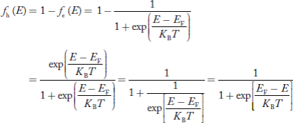
Hence, the Fermi-Dirac function of holes fh(E) in the valence band is:
|
Compared to exponential, the ‘1’ in the denominator is negligible,

Hence,
 ……….(21)
The density of hole states between E and E + dE in valence band can be written similar to Equation (8.9) for electrons.
 ……….(22)
Where mh* is the effective mass of the hole.
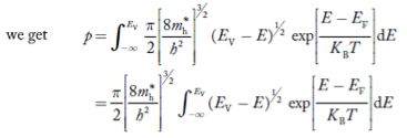
Substituting Equations (21) and (22) in (20),
|
……….(23)
The above equation can be simplified by the substitution:
Putɛ = EV − E ............. (24)
sodɛ = − dE
In Equation (24), EV is constant, as we change the variable E to ε in Equation (23), the integral limits also change.
In Equation (24),
as E → EV then ε → 0
and E→−∞, then ε →∞
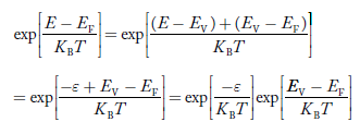
the exponential term in Equation (23) becomes:
|
............. (25)
Substituting Equations (24) and (25) in (23), we get:
|
………….(26)
From Equation (14), we know the integral value  T)3/2 put here and we get
|
………….(27)
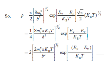
….The term is almost constant compared with the exponential term as the temperature changes. So, it is a pseudo constant and is given by the symbol NV. So, we have
|
…………… (28)
Key Takeaways
- The electrons in the conduction band behave as if they are free particles with effective mass me*
- The holes near the top of the valence band behave as if they are free particles with effective mass mh*.
- The density of Electrons in Conduction Band is given by n =Nc

- The density of Holes in Valence Band is given by p =Nv

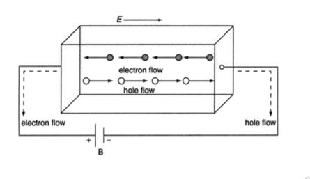
In semiconductor, the conduction band electron and valance band hole participate in electrical conduction. To obtain expression for electrical conductivity consider an intrinsic semiconductor bar which is connected to external battery as shown in figure
The electric field exist along x direction. The field accelerate electrons (conduction electrons) along negative X-direction and holes along positive X-direction. They starts moving with a constant velocity called Drift velocity vd
The total current in the semiconductor (due to both electron and hole)
I = Ie +Ih
or total current density
J = Je +Jh ..........(1)
|
Figure 11:Conductivity of semiconductors
In order to find the current density of electrons, let the concentration of electrons are 'n' , charge is 'e' and drift velocity is 've', Then
Je =neve ..........(2)
The drift velocity produced per unit electricfield is called 'mobility' , Thus
μe = 
or
μeE = 
substituting in equation 2
Je =neμeE ..........(3)
From Ohms law,
J = E where Je = eE
Je =neμeE = eE ..........(4)
e = neμe ..........(5)
Similarly current density for holes
Jp =peμpE = pE ..........(6)
And conductivity
p = peμp ..........(7)
Substituting value of Je and Jp from eq 4 and 6 in eq 1, we get
J =neμeE +peμpE
J =(neμe + peμp)E ..........(8)
From Ohms law J = E
= neμe + peμp
Where e = neμeandp = peμp
Also ni =CT3/2e -Eg/2kT ..........(9)
Therefore
= nie(μe + μp) =CT3/2e -Eg/2kTe(μe + μp) ..........(10)
The mobilities of carrier depend upon temperature as
μ
For Electronsμe
 and for holes μp

μe + μp= =
=  ..........(11)
Using equation 11 in equation 10
=CT3/2e -Eg/2kTe
=Ce e -Eg/2kT
Let B =Ce we get
=Be -Eg/2kT ..........(12)
Key Takeaways
- In semiconductor, the conduction band electron and valance band hole participate in electrical conduction.
- The electric field exist along x direction. The field accelerate electrons (conduction electrons) along negative X-direction and holes along positive X-direction. They starts moving with a constant velocity called Drift velocity vd
- The total current in the semiconductor is due to both electron and hole i.e.
I = Ie +Ih
- Current density is given as J = (neμe + peμp)E
- The mobilities of carrier depend upon temperature as μ

When the magnetic field is applied perpendicular to a current-carrying conductor, then a voltage is developed in the material perpendicular to both the magnetic field and current in the conductor. This effect is known as Hall Effect and the voltage developed is known as Hall voltage (VH).
Hall Effect is useful to identify the nature of charge carriers in material and hence to decide whether the material is an n-type semiconductor or p-type semiconductor, also to calculate carrier concentration and mobility of carriers.
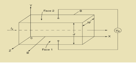
Hall Effect can be explained by considering a rectangular block of an extrinsic semiconductor in which current is flowing along the positive X-direction and magnetic field B is applied along Z-direction as shown in Figure.
|
Figure 12: Hall Effect
Suppose if the semiconductor is n-type, then mostly the carriers are electrons and the electric current is due to the drifting of electrons along negative X-direction or if the semiconductor is p-type, then mostly the carriers are holes and the electric current is due to drifting of the holes along positive X-direction.
As these carriers are moving in the magnetic field in the semiconductor that means they experience Lorentz force represented by FL
FL= Bevd
Where vd is the drift velocity of the carriers. (already explained in the previous section).
We can obtainthe direction of this force by applying Fleming’s left-hand rule in electromagnetism.
Fleming’s left-hand rule can be explained as If we stretch the thumb, forefinger, and middle finger in three perpendicular directions so that the forefinger is parallel to the magnetic field and the middle finger is parallel to the current direction, then the thumb represents the direction of the force on the current-carrying carriers.
So the Lorentz force is exerted on the carriers in the negative Y-direction. Due to Lorentz force, more and more carriers will be deposited at the bottom face (represented by face 1in the figure) of the conductor.
The deposition of carriers at the bottom face is continued till the repulsive force due to accumulated charge balances the Lorentz force.
After some time of the applied voltage, both the forces become equal in magnitude and act in opposite direction, then the potential difference between the top and bottom faces is equal to Hall voltage and that can be measured.
At equilibrium, the Lorentz force on a carrier
FL = Bevd ……………..(1)
and the Hall force
FH = eEH ……………..(2)
Where EH is the Hall electric field due to accumulated charge.
At equilibrium,FH = FL
eEH = Bevd
∴ EH = Bvd ……………..(3)
If ‘d’ is the distance between the upper and lower surfaces of the slab, then the Hall field
EH =  ……………..(4)
In n-type material, Jx = –nevd
vd = -  ……………..(5)
Where n is free electron concentration, substituting (5) in (3), we have
∴ EH = -B ……………..(6)
For a given semiconductor, the Hall field EH is proportional to the current density Jx and the intensity of magnetic field ‘B’ in the material.
i.e.EH ∝ JxB
(or)EH = RHJxB ……………..(7)
Where RH = Hall coefficient
Equations (6) and (7) are the same so, we have
RHJxB =-B
RH = - = -
= - ……………..(8)
Whereρ is the charge density
Similarly for p-type material
RH = =
= ……………..(9)
Using Equations (8) and (9), carrier concentration can be determined.
Thus, the Hall coefficient is negative for n-type material. In n-type material, as the more negative charge is deposited at the bottom surface, so the top face acquires positive polarity and the Hall field is along negative Y-direction. The polarity at the top and bottom faces can be measured by applying probes.
Similarly, in the case of p-type material, a more positive charge is deposited at the bottom surface. So, the top face acquires negative polarity and the Hall field is along positive Y-direction. Thus, the sign of the Hall coefficient decides the nature of (n-type or p-type) material.
The Hall coefficient can be determined experimentally in the following way:
Multiplying Equation (7) with ‘d’, we have
EHd = VH = RHJxBd ……………..(10)
From (Figure 12)we know the current density Jx
Jx = 
Where W is the width of the box. Then, Equation (10) becomes
VH = RH Bd = RH
RH =  ……………..(11)
Substituting the measured values of VH, Ix, B, and W in Equation(11), RH is obtained. The polarity of VH will be the opposite for n- and p-type semiconductors.
The mobility of charge carriers can be found by using the Hall effect, for example, the conductivity of electrons is
n= neμn
Or we can rewrite it as
μn =  =n RH ……………..(12)
by using equation(11)
μn = n ……………..(13)
Applications of Hall Effect
• Using magnetic flux leakage – To properly inspect items such as pipes or tubes, Hall Effect probes work with something called magnetic flux leakage. This is a way of testing such items, and being able to spot potential corrosion, erosion, or pitting. This is specifically used in steel items and can give important information about lifespan or safety.
• Sensors to detect rotation speed – A Hall Effect probe can be used in bicycle wheels, speedometers in the automotive world, electronic types of ignition systems, and gear teeth.
• Used to detected movement – You will often find a Hall Effect probe used in such items as Go-Kart controls, smartphones, paintball guns, or airsoft guns, as well as some GPS systems.
• Ferrite Toroid Hall Effect current transducers – This is mainly used in electronic compasses, making use of the magnetic field to show direction.
• Split-ring clamp-on sensors – These types of Hall Effect probes are used to test equipment without having to take the whole circuit board apart, e.g. complex items.
• Analog multiplication – Anything which needs a power measurement, e.g. sensing, and is also used in small computers.
• General power measurement – Any device which needs to be tested for its power input can be done by a Hall Effect probe.
• Position and motion sensors – This is mainly used in a DC motor, often the brushless type.
• The automotive world – Hall Effect probes are used widely in the automotive world, especially in fuel injection and ignition. Wheel rotation sensors also use Hall Effect probes, e.g. for anti-lock braking.
- For determination of the type of given semiconductor.
- For N-type, Hall coefficient RH= negative
- For P-type, Hall coefficient RH= Positive
- To determine carrier concentration n andp; that is n=p=1/e𝑅𝐻
- Determination of mobility of charge carriers μn =
 =n RH. Where 𝜎= electrical conductivity
 - To determine the sign of charge carriers whether the conductivity is due to electrons or holes.
Main Advantages of Using Hall Sensors
Why is a Hall Effect probe advantageous in all of these instances? Because the probes are not affected by outside influences, e.g. water or dirt. They can also easily sense the measure of the output they need when they are placed in the right position. On top of this, Hall Effect probes are safer, because the voltage never actually makes it directly to the sensor/probe. This makes this type of measurement overall so much safer than other methods.
As you can see, understanding how something is put into practice in the real world helps you to understand it in real terms. The Hall Effect is certainly very commonplace these days, in much more methods and applications than we realize. While certainly very useful in the automation world, even basic items such as a compass make large use of this scientific approach.
Key Takeaways
- When the magnetic field is applied perpendicular to a current-carrying conductor, then a voltage is developed in the material perpendicular to both the magnetic field and current in the conductor. This effect is known as Hall Effect.
- The voltage developed is known as Hall voltage (VH).
- Hall Effect is useful to identify the nature of charge carriers in material and hence to decide whether the material is an n-type semiconductor or p-type semiconductor.
- Hall Effect also to calculate carrier concentration and mobility of carriers.
- Hall coefficient is given by RH = -
 = -
= - Where ρ is the charge density
 - Hall coefficient is given by RH =

- Mobility of charge carriers can be found by using the Hall Effect μn = n

Definitions:
A dielectric is an electrical insulator that can be polarized by an applied electric field. Or
A dielectric is non-conducting material which stores electrical charges.
In other words, A material that does not conduct electricity but on applying electric field, induced charges produced on its faces. Such an insulator is called Dielectric.
Dielectrics are insulators i.e. non-conducting substances which are bad conductor of electric current. Dielectric materials can stores an electrostatic charge while dissipating minimal energy in the form of heat.
Examples of dielectric are Mica, Plastics, Glass, Porcelain and Various Metal Oxides and even dry air is also example of dielectric.The dielectric constant of a vacuum is, of course, unity.
Classification of Dielectric
The response of a dielectric material depends on the nature of its molecules. The molecules of a dielectric is of two types
- Polar molecules
- Non polar molecules
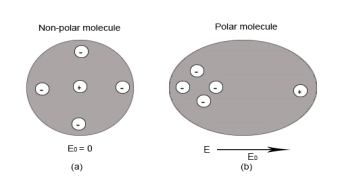
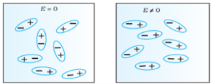
Polar Molecules: Polar Molecules are those in which centre of gravity of positive and negative charge does not coincide with each other. This is because they all are asymmetric in shape. Examples: H2O, CO2, NO2 etc.The moleculeof material are composed of two or more different atoms, which have permanently dipole momentbecause the centre of gravity of positive charge and negative charge does not coincide with eachother but separated by a finite (small) distance.
Normally this type of molecular dipole in polar dielectric are randomly oriented such that their net dipole moment becomes zero and material act as a neutral material.
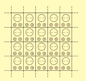
|
Figure 13:Effect of electric felid on dielectric
Polar Molecules are those type of dielectric in which the possibilities that the positive and negative molecules will coincide with each other is null or zero.
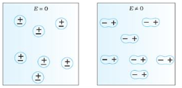
Non-Polar Molecule: Non-polar molecules are those in which centre of gravity of positive charge and negative charge coincide with each other. The molecule has zero dipole moment as they all are symmetric in shape. Examples: O2, N2, H2 etc.
Dielectrics materials in which the molecule's center of gravity of positive charge and negative charge coincide with eachotherand so the molecules are electrically neutral and hence zero dipole moment.
|
Figure 14: Polar molecules & Non polar molecules
Difference between Dielectric and Insulators
Dielectrics are often confused with insulators. Here are some points of differences
- Dielectric is the material which stores the electrical energy in an electric field whereas insulator is that material which blocks the flow of electrons.
- Dielectric material is polarised whereas insulator material doesn’t get polarised.
- Molecules in dielectric are weakly bounded as compared to molecules in insulator.
- Dielectric material has high dielectric constant whereas insulator has low dielectric constant.
- Examples of Dielectric material are dry air, vacuum,Glass, Porcelain, Various Metal Oxides and distilled water. Whereas Examples of insulator are cotton, plastic, rubber etc.
In dielectric material molecules are tightly bounded to the nucleus and not able to move freely as in case of conductor. But when a dielectric material is placed in an electric field, electric charges do not flow through the material as they flow in case of an electrical conductor but only slightly shift from their average equilibrium positions causing dielectric polarization. Because of dielectric polarization, positive charges are displaced in the direction of the field and negative charges shift in the direction opposite to the field. In dielectric molecules are tightly bound to the nucleus and not able to move freely as in case of conductors. The dielectric material is largely used in the manufacturing of capacitor.
Response of Dielectric to External Electric Field
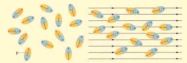
In case of Polar Molecules-When the electric field is not present, it causes the electric dipole moment of these molecules in a random direction. This is why the average dipole moment is zero. If the external electric field is present, the molecules align themselves in the direction electric field and resulted in having dipole moment.
In case of Non-Polar Molecules– As we know nonpolar molecule has zero dipole moment. In spite of zero dipole, when a dielectric nonpolar material is placed in an electric field. The positive and the negative charges in a nonpolar molecule experience forces in opposite directions. This force causes the separation between the charges and hence nonpolar molecule experiences induced dipole moment.
|
|
Figure 15 (a) (left) Non Polar Molecule Figure 15 (b) (right) Polar Molecule
Key Takeaways
- A dielectric is non-conducting material which stores electrical charges.
- Examples of dielectric are Mica, Plastics, Glass, Porcelain and Various Metal Oxides and even dry air is also example of dielectric.
- The molecules of a dielectric is of two typesPolar molecules and Non-polar molecules
- Polar Molecules are those in which centre of gravity of positive and negative charge does not coincide with each other.
- Non-polar molecules are those in which centre of gravity of positive charge and negative charge coincide with each other. The molecule has zero dipole moment as they all are symmetric in shape.
- In the presence of electric field molecules gets polarized.
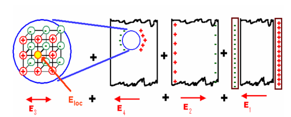
In dielectric solids, the atoms or molecules experience not only the external applied electric field but also the electric field produced by the dipoles. The resultant electric field acting on the atoms or molecules of dielectric substance is called the local field or an internal field.
To find an expression for local electric field on a dielectric molecule or an atom, we consider a dielectric material in the electric field of intensity E, between the capacitor plates so that the material is uniformly polarized, as a result opposite type of charges are induced on the surface of the dielectric near the capacitor plates. The local field is calculated by using the method suggested by Lorentz.
According to this method,
Internal field or Local field in solids
Consider a dielectric material and is subjected to external field of intensity E1. The charges are induced on the dielectric plate and the induced electric field intensity is taken as E2. Let E3 be the field at the center of the material. E4 be the induced field due to the charges on the spherical cavity. The total internal field of the material is
 ………..(1)
|
Figure 16: Local field in solids
Now consider the Electric field intensity applied E1
 ………..(2)
We know
 ………..(3)
Substituting the Electric flux density D in E1, we get
 ………..(4)
 ………..(5)
E2 is the Electric field intensity due to induced or polarized charges
 ………..(6)
Here the charge is induced due to the induced field so the electric flux density D changes to the electric polarization P
 ………..(7)
Since we have considered that the specimen is non-polar dielectric material, at the center of the specimen the dipole moment is zero and hence the electric field intensity at the center is zero due to symmetric structure.
 ………..(8)
Now consider a circle from the center of the dielectric material. Calculation of the electric field intensity E4 on the surface of spherical cavity.
As we know the polarization P is the induced charge per unit area
 ………..(9)
Here the polarization changes to its component so we will take the component which is contributing.

 ………..(10)
Now this equation can be solved by finding out the values of the charge dq in the surface are dA. We know the Electric field intensity E
 ………..(11)
Multiplying with the cosine angle on both the sides we get
 ………..(12)
Now by applying all the present condition for the above equation we
 ………..(13)
Now substituting the charge dq in the above equation we get
 ………..(14)
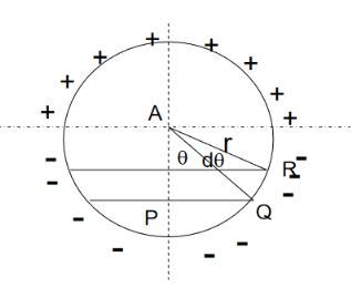
|
Figure 17:Sphere under applied field
If dA is the surface area of the sphere of radius rlying between θand θ+dθis the direction with reference to the direction of the applied force,then
dA= 2π(PQ)(QR) but sinθ= PQ/r, PQ = rsinθ ………..(15) and dθ=QR/r, QR=r dθ ………..(16)
Hence dA= 2πrsinθrdθ= 2πr2sinθdθ ………..(17) Now substituting all the values in the electric field intensity on the spherical cavity E4 we get,
Substituting (17) in (18), we get
Integrating with in the limits 0 to π
On solving the integration we get,
So the total electric field
Hence the Internal field obtained is
|
CLAUSSIUS -MOSOTTI EQUATION
It gives the relation between the dielectric constant and the ionic polarizability of atoms in dielectric material. If there are N number of atoms, the dipole moment per unit volume which is called Polarization is given by,
we know internal field
From above equations
we know polarization from the relation between polarization and dielectric constant
from the above two equations we get,
|
Key Takeaways
- In dielectric solids, the atoms or molecules experience not only the external applied electric field but also the electric field produced by the dipoles.
- The resultant electric field acting on the atoms or molecules of dielectric substance is called the local field or an internal field.
- The local field is calculated by using the method suggested by Lorentz.
- Internal field or Local field in solids is given by sum of external field of intensity, induced electric field intensities.
|
Dielectric materials are basically basic and pure electrical insulators. By applying a sensible electrical field, the dielectric gases can be polarised. Vacuum, Solids, Liquids and Gases can be a dielectric material.
Solid Dielectrics
They are electrical insulators. Effective electrical insulation is essential for any electronic device or electrical apparatus.
Their band gap energy is large, making them transparent to light of short wavelengths and creating the potential to serve as effective light-transmitting and light-emitting devices.
The first interesting fact about solids is that therecan be a permanent polarization which exists even without applying anelectric field. An example occurs with a material like wax, which contains longmolecules having a permanent dipole moment.
If you melt some wax and applied astrong electric field on it, this become liquid, so that the dipole moments get partiallylined up, they will stay that way when the liquid freezes.
The solid material willhave a permanent polarization which remains when the field is removed. Such asolid is called an electret.
|
Figure 18: A complex crystal lattice canhave a permanent intrinsic polarization P.
An electret has permanent polarization charges on its surface. It is theelectrical analogy of a magnet. It is not as useful, though, because free chargesfrom the air are attracted to its surfaces, eventually cancelling the polarizationcharges. The electret is “discharged” and there are no visible external fields.
A permanent internal polarization P is also found occurring naturally insome crystalline substances. In such crystals, each unit cell of the lattice has anidentical permanent dipole moment, as drawn in Figure 18.
For crystals that do not have a permanent moment, one can work out a theory of the dielectric constant that involves the electronic polarizability of the atoms.
Solid dielectrics are perhaps the most commonly used dielectrics in electrical engineering, and many solids are very good insulators. Some examples include porcelain, glass, and most plastics.
A wide range of different materials are used as solid dielectrics in high voltage plant. Although much use has been made of paper and oil as insulation, the tendency is now to move towards synthetic polymers. As a result, understanding the effects of temperature, mechanical loadings and electrical stresses on polymeric insulation is technologically important and presents numerous scientific challenges
Gaseous Dielectrics
A dielectric gas is also called as an insulating gas. It is a dielectric material in gaseous state which can prevent electrical discharge. Dry air, Sulphur hexafluoride (SF6) etc are the examples of gaseous dielectric materials.
Gaseous dielectrics are not practically free of electrically charged particles. When a peripheral electric field is applied to a gas, the free electrons are formed. These free electrons are accelerated from cathode to anode by the electric pressure applying a force on them.
When these electrons achieve adequate energy to bang off the electrons of the gas atoms or molecules and after that, the electrons are not involved by the molecules, and then the electron concentration will begin to build up exponentially. As a result, breakdown occurs.
A few gases such as SF6 are strongly attached (the electrons are powerfully attached to the molecule), some are weakly attached for e.g., oxygen and some are not at all attached for e.g. N2.
Examples of dielectric gases are Ammonia, Air, Carbon dioxide, Sulphur hexafluoride (SF6), Carbon Monoxide, Nitrogen, Hydrogen etc. The moisture content in dielectric gases may alter the properties to be a good dielectric
The mechanism of breakdown will directly depend on the nature of the dielectric gases and the electrode polarity in which the breakdown begins. If breakdown begins at cathode, then the supply of initiatory electrons is by the electrode itself. Then the electrons will get accelerates, numerous electrons formation occurs and it results in breakdown. If breakdown begins at anode, then the supply of initiatory electrons is by the gas itself. For e.g. air and SF6 gas. A tiny sharp point in a gas may also be the reason of breakdown of gas gap. This happens as a result of step-by-step breakdown processes.
Air, nitrogen and sulphur hexafluoride are the three most commonly used gaseous dielectrics.
Key Takeaways
- Vacuum, Solids, Liquids and Gases can be a dielectric material.
- Solid Dielectrics are electrical insulators. Effective electrical insulation is essential for any electronic device or electrical apparatus.
- Solid Dielectrics have their band gap energy is large, making them transparent to light of short wavelengths and creating the potential to serve as effective light-transmitting and light-emitting devices.
- A wide range of different materials are used as solid dielectrics in high voltage plant.
- Liquid dielectric is a dielectric material in liquid state. Its main purpose is to prevent or rapidly quench electric discharges.
- Liquid dielectrics are mixtures of hydrocarbons. They are weakly polarised. When used for electrical insulation they should be free from moisture, products of oxidation and other contaminants.
- A dielectric gas is also called as an insulating gas. It is a dielectric material in gaseous state which can prevent electrical discharge.
- Dry air, Sulphur hexafluoride (SF6) etc. are the examples of gaseous dielectric materials.
We can say that transformer is basic arrangement of conductors and dielectric insulators. Transformer is a static device consisting of two or more windings which comprehend a common magnetic field.
We know that transformer contains two parts: Primary coil and secondary coil. Energy transforms from primary coil to secondary coil only through magnetic induction, not by any electrical path. So to avoid electrical conduction we must use dielectric insulator at all possible places.
In transformer, the dielectric materials are used as insulator as well as cooling agents. Based on the applications of dielectric in transformer they fall into three groups.
1.Gaseous Dielectric in transformer.
2.Liquid dielectric in transformer.
3.Solid dielectric in transformer.
Gaseous Dielectric in Transformer
- The usage of nitrogen in transformer prevents oxidation and reduces the rate of deterioration.
- Sulphur hexafluoride dielectric is an electronegative gas which is used in transformer.
- It is non-toxic, non-inflammable and chemically inert.
Liquid Dielectric in Transformer
- Transformer oil - It is a class of mineral insulating oil and is used as a coolant.
- It also maintains the insulation of the winding.
- Fluorocarbon liquids are used in large transformer to give high heat transfer rates together with high dielectric strength.
Solid Dielectric in Transformer
- Fibrous materials are used in air cooled Transformers.
- Cotton tape is used for insulating the conductors of oil cooled transformers.
- High quality synthetic resin bonded paper in the form of cylinders is used as an insulator between core and coils and also between primary and secondary windings.
- Press board or press paper is used as a filling, and as a packing material between coils.
Key Takeaways
- Transformer is basic arrangement of conductors and dielectric insulators.
- Transformer contains two parts: Primary coil and secondary coil.
- Energy transforms from primary coil to secondary coil only through magnetic induction, not by any electrical path. So to avoid electrical conduction we must use dielectric insulator at all possible places.
- In transformer, the dielectric materials are used as insulator as well as cooling agents.
- Based on the applications of dielectric in transformer they fall into three groups:-Gaseous Dielectric in transformer, Liquid dielectric in transformer, Solid dielectric in transformer.
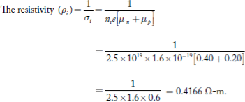
1 Question:Find the resistivity of an intrinsic semiconductor with intrinsic concentration of 2.5 × 10¹⁹ per m3. The mobilities of electrons and holes are 0.40 m2/ V-s and 0.20 m2/ V-s.
Solution:
Given data are:
Intrinsic concentration (ni) = 2.5 × 10¹⁹/m3
Mobility of electrons (μn) = 0.40 m2/V-s
The mobility of holes (μp) = 0.20 m2/V-s
The conductivity of an intrinsic semiconductor (σi) = nie[μn + μp]
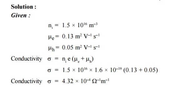
2 Question:The intrinsic carrier density is 1.5 × 10¹⁶ m–3. If the mobility of electron and hole are 0.13 and 0.05 m2 V–1 s–1, calculate the conductivity.
|
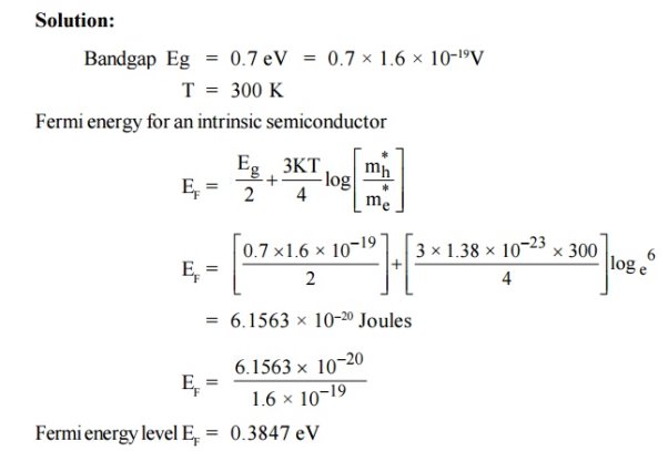
3 Question:For an intrinsic Semiconductor with a band gap of 0.7 eV, determine the position of EF at T = 300 K if m*h = 6m*e
Solution:
|
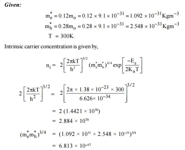
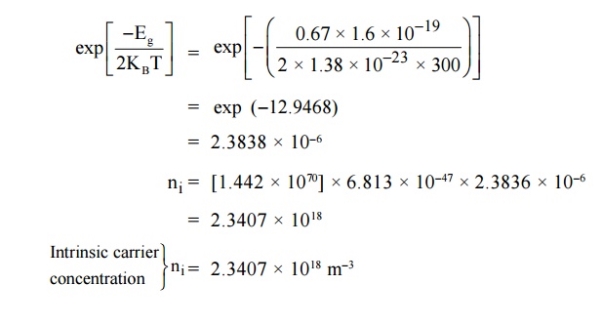
4 Question:Calculate the intrinsic concentration of charge carriers at 300 K given that m *e =0.12m o ,m*h =0.28mo and the value of brand gap = 0.67 eV.
Solution:
|
5 Question: The intrinsic carrier density is 1.5 × 10¹⁶ m–3. If the mobility of electron and hole are 0.13 and 0.05 m2 V–1 s–1, calculate the conductivity.
|
|
Reference
- Introduction to Solid State Physics -- Charles Kittel
- Solid State Physics-S 0 Pillai, 8th Ed New Age International Publishers-2018.
- Engineering physics- Gaur and Gupta, & S.Chand Publication
- Engineering physics - Avadhanalu and Kshirsagar, S.Chand Publication
