Question Bank
Unit 4
Q 1 What do you understand by intrinsic and extrinsic semiconductors?
Answer:
Intrinsic semiconductor
In an intrinsic semiconductor, even at room temperature, hole-electron pairs are created. When electric field is applied across an intrinsic semiconductor, the current conduction takes place by two processes, namely; by free electrons and holes. The free electrons are produced due to the breaking up of some covalent bonds by thermal energy. At the same time, holes are created in the covalent bonds. Under the influence of electric field, conduction through the semiconductor is by both free electrons and holes. Therefore, the total current inside the semiconductor is the sum of currents due to free electrons and holes.

Extrinsic semiconductor
The amount and type of such impurities have to be closely controlled during the preparation of extrinsic semiconductor.
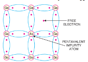
Generally, for 108 atoms of semiconductor, one impurity atom is added. The purpose of adding impurity is to increase either the number of free electrons or holes in the semiconductor crystal. As we shall see, if a pentavalent impurity (having 5 valence electrons) is added to the semiconductor, a large number of free electrons are produced in the semiconductor. On the other hand, addition of trivalent impurity (having 3 valence electrons) creates a large number of holes in the semiconductor crystal. Depending upon the type of impurity added,
Extrinsic semiconductors are classified into:
(i) n-type semiconductor
(ii) p-type semiconductor

Q 2 What do you mean by fermi level? Explain
Answer:
The highest energy level that an electron can occupy at the absolute zero temperature is known as the Fermi Level. The Fermi level lies between the valence band and conduction band because at absolute zero temperature the electrons are all in the lowest energy state.
In a p type semiconductor, there is an increase in the Density of unfilled States. Thus, more electrons can be accommodated at lower energy states. In a n type semiconductor, the DOS is increased. Thus, electrons have to be accommodated at higher energy levels.
Fermi level is also defined as the work done to add an electron to the system. More positive (more holes) in a p type semiconductor, mean lesser work needs to be done. Hence a lower Fermi level
When the material is at a temperature higher than OK, it receives thermal energy from surroundings i.e. electrons are thermally excited. As a result, they move into the higher energy levels which are unoccupied at OK. The occupation obeys a statistical distribution called Fermi – Dirac distribution law.
According to this distribution law, the probability F(E) that a given energy state E is occupied at a temperature T is given by

Here F(E) is called Fermi – Dirac probability function. It indicates that the fraction of all energy state (E) occupied under thermal equilibrium ‘K’ is Boltzmann constant.
Q 3 How pn junction diode work?
Answer:
When a layer of P - type semiconducting material is placed with a layer of N- type semiconducting material in such a way that the atoms of P-type combine with the atoms of N-type across the surface of contact, such a surface junction where combination has occurred is known as PN junction.
Combined p-type and n-type semiconductors with PN junction formation is known a junction diode or PN diode
Biased pn junction diode by diffusion technique:
Diffused junctions are formed by impurity diffusion technique. The diffusion process employs either gas diffusion method or solid diffusion method for example in gas diffusion method a wafer of n-type silicon is heated at about 10000 c in a gaseous atmosphere of high concentration gradient the boron atoms.
At the temperature due to concentration gradient the boron atom diffuses in to silicon forming p-n junction in solid diffusion process a p-type impurity (say indium) is painted on a n-type substrate and both are heated. Now impurity atoms diffuse into n-type substrate for a short distance and form p-n junction.

*The formation PN junction is represented in a figure. Let us consider the formation of a sharp junction when two separate semiconductors of p and n type are brought together.
* The p-type has holes as majority carriers and electrons as minority carriers while n-type has electrons as majority carries and holes as minority carriers.
* When they are joined, in the region of contact the free electrons diffuse from n-region and combine with holes in p-region. This leaves n-region near the boundary positively charged and p-region negatively as a result, electric field EB appears in a small region W on either side of the junction O. This region is called “Depletion region “. The thickness of this region is in the older of 6 ×10⁻⁶ cm.
* Due to electric field E B potential difference appears across the depletion region and this potential VB is called “Contact Potential or Barrier Potential or Junction Barrier”.
Q 4 Describe diffusion current?
Answer:
Diffusion current:
The flow of electric current due to the motion of charge carriers under concentration
Gradient is called diffusion current
Or
The motion of charge carriers from the region of higher concentration to lower
Concentration leads to a current called diffusion current.
Let be the excess electron concentration. Then according to Fick’s law, the rate of
Diffusion of charge carriers is proportional to concentration gradient is

Hence
Rate of diffusion of charge:

Where D is the diffusion coefficient of charge carriers
The negative sign indicates decrease of N with increase of x
So, the diffusion current density Jdiffuis:

Q.5 Define drift velocity?
Answer:
The flow of electric current due to the motion of charge carriers under the
Influence of external electric field is called drift current.
When an electric field E is applied across a semiconductor material, the charge
Carriers attain a drift velocity vd.
So, drift velocity
Vd=µE----------------(1)
The relation between current density J and drift velocityvdis
J=Nqvd
Where N is the carrier concentration
q is the charge of electron or hole
From equations (1) and (2), we get

_ is the mobility of charge carrier.
The above equation shows the general expression for drift current density.
Drift current density due to electrons is

Where is the electrons carrier concentration and
µe the mobility of electrons
Drift current density due to holes is

Q 6 What is photo cell?
Answer:
It is a form of light-weight sensor that converts light energy into electrical voltage or current. Photodiode is a type of semi conducting device with PN junction. Between the p (positive) and n (negative) layers, an intrinsic layer is present. The photo diode accepts light energy as input to generate electric current.
Typical photodiode materials are Silicon, Germanium, Indium Gallium Arsenide Phosphide and Indium gallium arsenide.
Internally, a photodiode has optical filters, built in lens and a surface area. When surface area of photodiode increases, it results in more response time. Few photo diodes will look like Light Emitting Diode (LED). It has two terminals . The smaller terminal acts as cathode and longer terminal acts as anode.
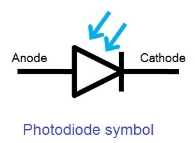
The symbol of the photodiode is similar to that of an LED but the arrows point inwards as opposed to outwards in the LED. The following image shows the symbol of a photodiode.

Q 7 What is equation of conductivity?
Answer:
The current is addition of two current , current  due to flow of holes and current
  due to flow of electron
So 
We will calculate conductivity due to flow electron only
E = electric field vector across the small section (in cylindrical form) of semiconductors
N= number of electron in above semiconductor
A= cross sectional area
L= length of section of cylindrical semiconductor
Let one electron contains charge q than total charge flow will be = Nq
So current flow due to electron will be
 = (Total charge flow)/(time taken in flow of charge)
 =
= 
Time  = (Average distance covered by electron) / (drift velocity of electron)
 =
= 
From above equation
- =

- Let conduction current density due to flow of current (due to flow of electron ) is
 , and we know that
 =
= 
From above equation

= 
 =
= 
Where  =
=  = number of electrons per unit volume
Drift velocity of electron can be expressed as
 =
= 
Where  is mobility of electron
Q 8 What is LED?
Answer:
Light Emitting Diodes (LEDs) are the most widely used semiconductor diodes among all the different types of semiconductor diodes available today. Light emitting diodes emit either visible light or invisible infrared light when forward biased. The LEDs which emit invisible infrared light are used for remote controls
When Light Emitting Diode (LED) is forward biased, freeelectrons in the conduction band recombines with the holes in the valence band and releases energy in the form of light.
The process of emitting light in response to the strong electricfield or flow of electric current is called electroluminescence.
A normal p-n junctiondiode allows electric current only in one direction. It allows electric current when forward biased and does not allow electric current when reverse biased. Thus, normal p-n junction diode operates only in forward bias condition.
Light Emitting Diode (LED) works only in forward bias condition. When Light Emitting Diode (LED) is forward biased, the free electrons from n-side and the holes from p-side are pushed towards the junction.
When free electrons reach the junction or depletion region, some of the free electrons recombine with the holes in the positive ions. We know that positive ions have less number of electrons than protons. Therefore, they are ready to accept electrons. Thus, free electrons recombine with holes in the depletion region. In the similar way, holes from p-side recombine with electrons in the depletion region.
Q 9 Define Hall Effect?
Answer:
When a material carrying current is subjected to a magnetic field in a direction perpendicular to direction of current, an electric field is developed across the material in a direction perpendicular to both the direction of magnetic field and current direction. This phenomenon is called “Hall-effect”.
Explanation:
* Consider a semi-conductor, and current passes along the X-axis and a magnetic field Bz is applied along the Z-direction, a field Ey is called the Hall field which is developed in the Y-direction.
*In P-type semi-conductor, holes move with the velocity “V” in the “+”ve X-direction. As they move across the semiconductor the holes experience a transverse force ‘Bev’ due to the magnetic field.
* This force drives the holes down to the lower face. As a result, the lower face becomes +vely charged and –ve charge on the upper surface creating the hall field in the Y-direction. The Hall field exerts an upward force on holes equal to Ee.
* In the steady sate, two forces just balance and as a result, no further increase of + ve charge occurs on Face1.
* In N type semiconductor, the majority charge carriers are electrons experiences a force in the downward direction and lower face gets – vely charged. As a result, Hall field will be in the Y – direction.

Hall Coefficient:
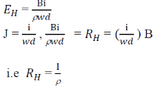
Hall field𝐸𝐻, for a given material depends on the current density J and the applied magnetic field B.
i.e. 𝐸𝐻α JB
𝐸𝐻= 𝑅𝐻α JB
Since,

This is called hall coefficient.
Q 10 What is carrier construction?
Answer:
Negative charge carriers (Electron)
The negative charge carriers such as free electrons are the charge carriers that carry negative charge with them while moving from one place to another place. Free electrons are the electrons that are detached from the parent atom and moves freely from one place to another place.

Positive charge carriers (Holes)
The positive charge carriers such as holes are the charge carriers that carry positive charge with them while moving from one place to another place. Holes are the vacancies in valence band that moves from one place to another place within the valence band.
The charge carriers that are present in large quantity are called majority charge carriers. The majority charge carriers carry most of the electric charge or electric current in the semiconductor. Hence, majority charge carriers are mainly responsible for electric current flow in the semiconductor.
The charge carriers that are present in small quantity are called minority charge carriers. The minority charge carriers carry very small amount of electric charge or electric current in the semiconductor.
Charge carriers in intrinsic semiconductor
The semiconductors that are in pure form are called intrinsic semiconductors. In intrinsic semiconductor the total number of negative charge carriers (free electrons) is equal to the total number of positive charge carriers (holes or vacancy).
Total negative charge carriers = Total positive charge carriers