Unit I
Diode Circuits
Forward biased

Figure 2. Forward biased PN junction
In forward biased p-n junction diode since the anode terminal is a positively charged electrode or conductor, which supplies holes to the p-n junction. The anode terminal or positive terminal is the source of positive charge carriers (holes), the positive charge carriers (holes) begins their journey at anode terminal and travel through the diode and ends at cathode terminal.
Reverse bias

Figure 3. Reverse Biased PN junction
When the diode is reverse biased the anode terminal becomes negative and cathode terminal becomes positive. The anode terminal is the source of free electrons. The free electrons begin their journey at the anode terminal and fill large number of holes in p-type semiconductor.
The holes in p-type semiconductor get attracted towards the negative terminal. The free electrons from negative terminal cannot move towards the positive terminal because the wide depletion region at p-n junction opposes the flow of electrons.
The cathode terminal is the source for holes, the holes begin their journey at the cathode terminal and occupy the electrons in n-type semiconductor. The free electrons in the n-type semiconductor gets attracted towards the positive terminal.
The holes from the positive terminal cannot move towards the negative terminal because the wide depletion region at the p-n junction opposes the flow of holes.
Advantages:
2. Explain the V-I characteristics of diode ?
Forward Bias
When positive supply voltage is applied the electrons get enough energy to overcome the potential barrier and cross the junction. This is applicable to holes. The amount of energy required for electrons and holes for crossing the potential barrier is 0.3V for Ge and 0.7 V for Si, and 1.2 V for GaAs. This is known as Voltage drop. The voltage drop across the diode occurs due to internal resistance.


Figure 4. Forward V-I characteristics of diode
The slope of the PN junction diode in forwarding bias shows that resistance is very low. When a forward bias is applied to the diode then it causes a low impedance path and permits to conduct a large amount of current which is known as infinite current. This current start to flow above the knee point with a small amount of external potential.
Reverse Bias
The current in this biasing is low till breakdown is reached and hence the diode looks like an open circuit. When the input voltage of the reverse bias has reached the breakdown voltage, reverse current increases enormously.
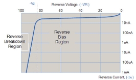

Figure 5. V-I characteristics of diode in reverse bias.
When the reverse voltage is increased beyond the limit, then the reverse current increases drastically. This particular voltage that causes the drastic change in reverse current is called reverse breakdown voltage. Diode breakdown occurs by two mechanisms: Avalanche breakdown and Zener breakdown.
I = IS[exp ( qV/kT )-1]
K – Boltzmann Constant
T – Junction temperature (K)
(kT/q) Room temperature = 0.026V
Therefore, it can be written as
I=IS[exp(V/0.026)-1]

Figure 6. VI characteristics of diode in forward and reverse bias.
3. Explain half wave rectifier ?
A rectifier is a device that converts alternating current (AC) to direct current (DC).
A half wave rectifier is defined as a type of rectifier that only allows one half-cycle of an AC voltage waveform to pass, blocking the other half-cycle. Half-wave rectifiers are used to convert AC voltage to DC voltage. 
Figure 7. Half wave rectifier circuit and output waveforms.
During the positive half cycle of AC voltage, diode is forward biased and current flows through the diode.
During the negative half cycle of AC voltage diode is reverse biased and the flow of current is blocked.
In order to understand this concept, let us replace the secondary transformer coils with source voltage, hence the circuit diagram looks like this

Figure 8. Half wave rectifier with Ac voltage circuit.
Hence for positive half cycle of the AC source voltage, the equivalent circuit becomes:

Figure 9. Closed circuit
This is because the diode is forward biased and is hence allowing current to pass through.
But for the negative half cycle of the AC source voltage, the equivalent circuit becomes:

Figure 10. Open circuit
Because the diode is now in reverse bias mode, no current is able to pass through it. Since current cannot flow through to the load during this time, the output voltage is equal to zero.
Hence, the input and output voltage waveforms are shown in the figure.

Figure 11. Input and Output voltage waveforms of Half wave Rectifier.
4. Explain half-wave rectifier with capacitor filter ?
The output waveform obtained is a pulsating DC waveform. This is has been obtained without a filter. Filters are components used to convert smoothen pulsating DC waveforms into constant DC waveforms. They achieve this by suppressing the DC ripples in the waveform.
The circuit diagram below shows how a capacitive filter is can be used to smoothen out a pulsating DC waveform into a constant DC waveform.

Figure 12. Half wave rectifier with capacitor filter
Ripple Factor of Half Wave Rectifier
‘Ripple’ is the unwanted AC component remaining when converting the AC voltage waveform into a DC waveform. Even though we try out best to remove all AC components, there is still some small amount left on the output side which pulsates the DC waveform. This undesirable AC component is called ‘ripple’.
The ripple factor is the ratio between the RMS value of the AC voltage on the input side and the DC voltage on the output side of the rectifier.
 = [ (Vrms/ VDC ) 2 – 1 ] ½
Ripple factor = (I2 rms – I2 dc)/ Idc = 1.21
Rectifier efficiency (η) is the ratio between the output DC power and the input AC power. The formula for the efficiency is equal to:
η =Pdc/Pac
The efficiency of a half wave rectifier is equal to 40.6%
RMS value of Half Wave Rectifier
To derive the RMS value of half wave rectifier, we need to calculate the current across the load.
If the instantaneous load current is equal to iL = Imsinωt, then the average of load current (IDC) is equal to:

Where Im is equal to the peak instantaneous current across the load (Imax). Hence the output DC current (IDC) obtained across the load is:
Idc = Imax/π .where Imax = maximum amplitude of dc current.
For a half-wave rectifier, the RMS load current (Irms) is equal to the average current (IDC) multiple by π/2. Hence the RMS value of the load current (Irms) for a half wave rectifier is:
Irms = Im/2
Where Im= Imax which is equal to the peak instantaneous current across the load.
Peak Inverse Voltage of Half Wave Rectifier
Peak Inverse Voltage (PIV) is the maximum voltage that the diode can withstand during reverse bias condition. If a voltage is applied more than the PIV, the diode will be destroyed.
Form Factor of Half Wave Rectifier
Form factor (F.F) is the ratio between RMS value and average value,
F.F = rms value / Average value
The form factor of a half wave rectifier is equal to 1.57 .
Applications of Half Wave Rectifier
Advantages of Half Wave Rectifier
Disadvantages of Half Wave Rectifier
5. Explain the working of full wave rectifier ?
A full wave rectifier converts both halves of each cycle of an alternating wave AC signal into pulsating DC signal.

Figure 13. Full wave rectifier circuit diagram.
Centre-tapped Transformer: – It is a normal transformer with one slight modification. It has an addition wire connected to the exact centre of the secondary winding. This type of construction divides the AC voltage into two equal and opposite voltages namely +Ve voltage (Va) and -Ve voltage (Vb). The total output voltage is
V = Va + Vb

Figure 14. Full wave rectifier circuit operation.

Figure 15. During positive and negative half cycle.
We apply an AC voltage to the input transformer.
During the positive half-cycle of the AC voltage, terminal 1 will be positive, centre-tap will be at zero potential and terminal 2 will be negative potential. This will lead to forward bias in diode D1 and cause current to flow through it. During this time, diode D2 is in reverse bias and will block current through it.

Figure 16. During positive half cycle
During the negative half-cycle of the input AC voltage, terminal 2 will become positive with relative to terminal 2 and centre-tap. This will lead to forward bias in diode D2 and cause current to flow through it. During this time, diode D1 is in reverse bias and will block current through it.

Figure 17. During negative half cycle
During the positive cycle, diode D1 conducts and during negative cycle diode D2 conducts and during positive cycle. As a result, both half-cycles are allowed to pass through. The average output DC voltage here is almost twice of the DC output voltage of a half-wave rectifier.

6. Explain full wave rectifier with capacitive filter ?
Full wave rectifier filter circuit

Figure 19. Circuit diagram with filter circuit
In centre-tapped full wave rectifier lot of ripples are obtained at pulsating DC voltage. This cannot be used for practical applications. Hence, to convert pulsating DC voltage to pure DC voltage filter circuit is shown.
A capacitor is placed across the load. The working of capacitive filter circuit is short for ripples and block DC component so that it flows through another path and is available across the load.
During the positive half-wave, the diode D1 starts conducting. The capacitor is uncharged, and when we apply an input AC voltage which happens to be more than the capacitor voltage, it charges the capacitor immediately to the maximum value of the input voltage. At this point, the supply voltage is equal to capacitor voltage

Figure 20. Output waveforms with capacitive filter.
When the applied AC voltage starts decreasing and less than the capacitor, the capacitor starts discharging slowly but this is slower when compared to the charging of the capacitor and it does not get enough time to discharge entirely and the charging starts again.
So around half of the charge present in the capacitor gets discharged. During the negative cycle, the diode D2 starts conducting, and the above process happens again. This will cause the current to flow through the same direction across the load.
Ripple Factor (γ)
The output consist of both AC and DC components. The AC components are undesirable to us and will cause pulsations in the output. This unwanted AC components are called Ripple.
The expression ripple factor is given above where Vrms is the RMS value of the AC component and Vdc is the DC component in the rectifier.
For centre-tapped full-wave rectifier, we obtain γ = 0.48
Rectifier Efficiency (η)
Rectifier efficiency is the ratio between the output DC power and the input AC power.
For centre-tapped full-wave rectifier, ηmax = 81.2%
Form Factor (F.F)
The form factor is the ratio between RMS value and average value.
FF= RMS value/ Average value
For centre-tapped full wave rectifier, FF = 1.11
Advantages of Full Wave Rectifiers
Disadvantages of Full Wave Rectifiers
7. Explain the construction and working of Zener diode?

Figure 21. Zener Diode characteristics.
For operation in reverse bias Vz is positive on cathode and negative on anode. The forward characteristics are the same as forward biased p-n junction diode.
The values Vz, Iz(min), Iz(max) are the characteristics of diode.
Zener diode parameters:
It is the reverse bias voltage at which the Zener diode enters breakdown region maintaining a constant voltage Vz across the diode.
2. Minimum Reverse current(Izk)
It is the reverse current at the knee of reverse characteristics and is the minimum reverse current to sustain the breakdown condition.
3. Maximum Zener current(Izm)
It is the maximum current on the diode that can carry without exceeding the maximum power dissipation
4. Maximum Power Dissipation
It is the maximum power which the Zener diode can dissipate without destruction. It is given by the product of
Pd = Vz Izm
5. Dynamic Impedance
It defines how Vz changes with variations in diode reverse current. It is defined as
Zz = ∆ Vz / ∆ Iz
Applications:
8. Explain series clipper ?
Series clipper:
A half-wave rectifier is considered as a clipper because it passes only half cycle and clips the other half cycle of the input. Therefore, series clipper is known as half-wave rectifier circuit.
Series negative clipper
In series negative clipper, the negative half cycles of the input AC signal is removed at the output. The circuit construction of the series negative clipper is shown in the figure.

Figure 22. Negative series clipper
If the diode is arranged in such a way that the arrowhead of the diode points towards the output and the diode is in series with the output load resistance, then the clipper is said to be a series negative clipper.
During the positive half cycle of input,
Vi = Vm (>Vf)
Vf is the forward bias voltage required for the diode to conduct. For silicon diode Vf = 0.7 V .
The diode conducts and the current flows into R1.
Applying KVL to the path consisting of vi , Vf and vo when diode is conducting we have
Vi -Vf -vo =0 --------------------(1)
Vo = vi – Vf
Since vi= Vm we have
Vo = Vm – Vf ------------------------(2)
Note that the output voltage vo is less than the input voltage amplitude Vm by an amount Vf.
During the negative half cycle of input
Vi = -Vm (<Vf)
The diode is reverse biased and only the reverse saturation current Ir flows through R1.
Hence , vo = -Ir R1
Since Ir is very small , vo ≈ 0 .
During the positive half cycle, the diode D is forward biased during the positive half cycle.
During the negative half cycle, the diode D is reverse biased during the negative half cycle.
During reverse biased condition, no current flows through the diode. So, the negative half cycle is completely blocked or removed at the output. In other words, a series of negative half cycles are removed at the output.
Series negative clipper with bias
Sometimes it is desired to remove a small portion of positive or negative half cycles of the input AC signal. In such cases, the biased clippers are used.
The construction of the series negative clipper with bias is almost similar to the series negative clipper. The only difference is an extra element called battery is used in series negative clipper with bias.
Series negative clipper with positive bias

During the positive half cycle, the positive terminal A is connected to p-side and the negative terminal B is connected to n-side the diode is forward biased. However, we are also supplying the voltage from another source called battery. The positive terminal of the battery is connected to n-side and the negative terminal of the battery is connected to p-side of the diode.
That means the diode is forward biased by input supply voltage Vi and reverse biased by battery voltage VB. Initially, the battery voltage is greater than the input supply voltage. Hence, the diode is reverse biased and does not allow electric current. Therefore, no signal appears at the output.
When the input supply voltage Vi becomes greater than the battery voltage VB, the diode is forward biased and allows electric current. As a result, the signal appears at the output.
During the negative half cycle, the diode is reverse biased by both input supply voltage Vi and battery voltage VB. Therefore, during the negative half cycle, no signal appears at the output.
Series negative clipper with negative bias
During the positive half cycle, the diode D is forward biased by both input supply voltage Vi and the battery voltage VB. Therefore, during the positive half cycle, the signal appears at the output.

During the negative half cycle, the diode D is reverse biased by the input supply voltage Vi and forward biased by the battery voltage VB. Initially, the input supply voltage Vi is less than the battery voltage VB. So, the diode is forward biased by the battery voltage VB. As a result, the signal appears at the output.
When the input supply voltage Vi becomes greater than the battery voltage VB, the diode will become reverse biased. As a result, no signal appears at the output.
9. Explain dual clipper ?
Sometimes it is desired to remove a small portion of both positive and negative half cycles. In such cases, the dual clippers are used.
The dual clippers are made by combining the biased shunt positive clipper and biased shunt negative clipper.

During the positive half cycle, the diode D1 is forward biased by the input supply voltage Vi and reverse biased by the battery voltage VB1. On the other hand, the diode D2 is reverse biased by both input supply voltage Vi and battery voltage VB2.
Initially, the input supply voltage is less than the battery voltage. So, D1 is reverse biased by the battery voltage VB1. Similarly, the diode D2 is reverse biased by the battery voltage VB2. As a result, the signal appears at the output.
However, when the input supply voltage Vi becomes greater than the battery voltage VB1, the diode D1 is forward biased by the input supply voltage. As a result, no signal appears at the output.
During the negative half cycle, the diode D1 is reverse biased by both input supply voltage Vi and battery voltage VB1. Diode D2 is forward biased by the input supply voltage Vi and reverse biased by the battery voltage VB2.
Initially, the battery voltage is greater than the input supply voltage. Therefore, the diode D1 and diode D2 are reverse biased by the battery voltage. As a result, the signal appears at the output.
When the input supply voltage becomes greater than the battery voltage VB2, the diode D2 is forward biased. As a result, no signal appears at the output.
Applications of clippers
10. A positive series clipping circuit has ± 7V input and zero load current. Calculate a suitable resistor for R1 and specify the diode. Sketch the output voltage waveform.
Solution:
When diode conducts
Vo = -[Vm – Vf]
Assuming silicon diode
Vf = 0.7 V
Also Vm = 7V
Vo = -[7V – 0.7 V ] = - 6.3 V
R1 = vo/ If
= 6.3 / 1mA = 6.3 kΩ
Vr = Vm = 7V
Diode Specification
Vr = 7V
If = 1mA
The positive series clipper along with input and output waveforms is shown below.

11. Explain clamping circuits?
Clamping circuits are used to add or insert dc voltage level to a signal. A clamping circuit is called dc restorer since the dc voltage level lost in a signal can be recovered or restored by passing it through the clamping circuit.
Clamping operations can be understood with the following illustrations
In the figure a 5V dc is added to a signal peak value of 5V. The resulting signal is completely positive, and its negative peak is clamped to zero volts. The operation is positive voltage clamping.

In the figure -5V dc is added to a signal of peak value of 5V. The resulting signal is completely negative, and its positive peak is clamped to zero volts. The operation is called negative voltage clamping.

Negative voltage clamping circuit:

During the positive half cycle of input vi = Vm. The diode conducts and the charges the capacitor to Vm making the left plate positive.
Since the diode is connected between the output terminals
Vo = Vf
Applying KVL to the path consisting of vi,vc and VF we have
Vi – vc -Vf =0
Using vi = Vm we have
Vc = Vm -Vf
During the negative half cycle of the input vi = -Vm. The diode is reverse biased. The capacitor discharges into R!. The discharge is minimal as R1 is very high resistance. Hence, the capacitor voltage remains almost constant at
Vc = Vm – Vf
Apply KVL to the path consisting of vi,vc and vo we have
Vi – vc – vo = 0
Using vi = -Vm and vc Vm -Vf we get
Vo = -(2Vm -Vf)
Peak to peak output voltage is
Vo(p-p) = VF – [-(2Vm -Vf)]
= 2Vm
Peak to peak input voltage is
Vi(p-p) = Vm –(-Vm)
= 2Vm
Therefore, vo(p-p) = vi(p-p)
Positive voltage clamping circuit

During the negative half cycle of the input signal vi = -Vm . The diode conducts and charges the capacitor to Vm making the right plate positive.
Since the diode is connected between the output terminals and the polarities of VF and Vo are opposite we have
Vo = -VF
Applying KVL to the path consisting of vi,vc and VF we have
Vi +vc + VF =0
Using vi = -Vm we have
Vc = vm -VF
During the positive half cycle of the input vi = -Vm. The diode is under reverse bias. The capacitor discharges into R1 is a very high resistance the discharge is minimal. Hence, the capacitor voltage remains almost constant at
Vc = Vm – VF
Apply KVL to the path consisting of vi,vc and vo we have
Vi + Vc -Vo =0
Using vi = Vm and vc = Vm-VF we have
Vm +Vm -Vf -vo =0
Or vo = 2Vm -Vf
Peak to peak output voltage
Vo(p-p) = (2Vm -Vf) –(-Vf)
= 2 Vm
Peak to peak input voltage is
Vi(p-p) = Vm –(-Vm)
= 2 Vm
Observe that vo(p-p) = vi(p-p)
The output waveform is completely positive with its negative peak clamped at -VF . Hence, the circuit is known as positive voltage clamping circuit.
12.The input to the negative clamping clamping circuit is as shown in the figure which is at ±12V , 1kHz square wave . If R1= 47kΩ and C1 = 1µF. Calculate the tilt in the output waveform . Draw the circuit and sketch the input and output waveform.
Solution :
Vm = 12V f = 1kHz T = 1/f = 1msec. R1 = 47kΩ and C1 = 1µF.
The tilt in the waveform is given by
∆ vc = Ic x t / C1
Ic ≈ vo(p-p) / R1 = 2Vm /R1 =24 / 47 k = 510.64 µ A.
t=T/2 = 0.5 ms = 500 µ s
∆ vc = 510.64 µ x 500 µ / 1 µ = 255.32 mV.


