MP
Unit-28051 hitecture Q1) Explain the internal block diagram of 8051?A1)
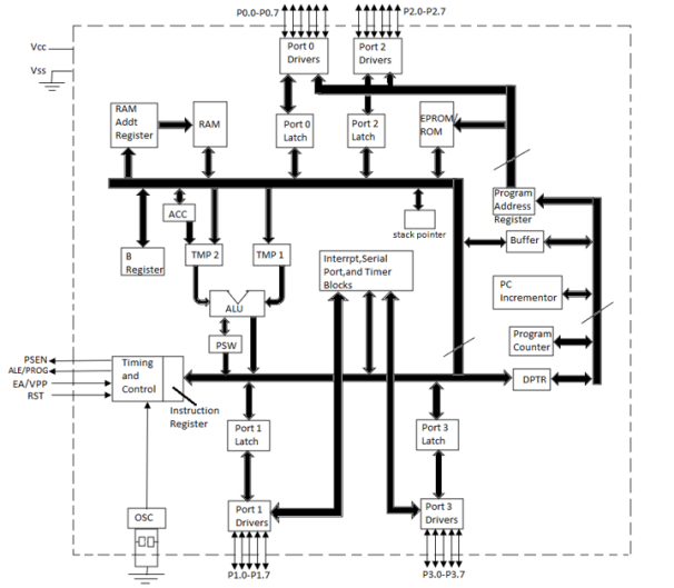
Figure 1. Internal Block Diagram8051 microcontroller was designed by Intel in 1981. It is an 8-bit microcontroller. It is built with 40 pins DIP (dual inline package), 4kb of ROM storage and 128 bytes of RAM storage, 2 16-bit timers. It consists of are four parallel 8-bit ports, which are programmable as well as addressable depending on the requirement. An on-chip crystal oscillator is integrated in the microcontroller having crystal frequency of 12 MHz. 8051 has 4 K Bytes of internal ROM. The address space is from 0000 to 0FFFh. If the program size is more than 4 K Bytes 8051 will fetch the code automatically from external memory. Accumulator is an 8 bit register widely used for all arithmetic and logical operations. Accumulator is also used to transfer data between external memory. B register is used along with Accumulator for multiplication and division. A and B registers together is also called MATH registers. PSW (Program Status Word). This is an 8 bit register which contains the arithmetic status of ALU and the bank select bits of register banks Q2) Write a short note on CPU and ALU?A2)CPU is the brain of any processing device of the microcontroller. It monitors and controls all operations that are performed on the Microcontroller units. It reads program written in ROM memory and executes them and does the expected task of that application.All arithmetic and logical functions are carried out by the ALU.
Addition, subtraction with carry, and multiplication come under arithmetic operations.
Logical AND, OR and exclusive OR (XOR) come under logical operations.
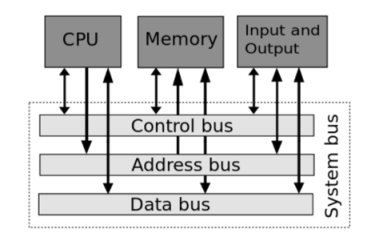
Q3) Explain address, data and control bus?A3)Basically, Bus is a collection of wires which work as a communication channel or medium for transfer of Data. There are three internal buses associated with processors: the data bus, address bus, and control bus. Together, these three make up the “system bus.”
Figure. Internal System BusControl Bus:Control signals move out of the processor, but not in to it.Address and Data bus:The data bus “width” of an MCU is typically 8-, 16-, 32- or 64-bits. The width of the data bus reflects the maximum amount of data that can be processed and delivered at one time. A 64-bit processor has a 64-bit data bus and can communicate 64-bits of data at a time, and whether the data is read or written is determined by the control bus. The physical location of the data in memory is carried by the address bus. An internal hardware component, having received the address from the address bus and about to receive the data, enables a buffer to allow the flow of signals to or from the location that was designated by the address bus. The address bus carries only the information regarding the address and is synchronized with the data bus to accomplish read/write tasks from the processor. The address bus is only as wide as is necessary to address all memory in the system. Q4) Write a short note on working registers?A4)General Purpose Registers
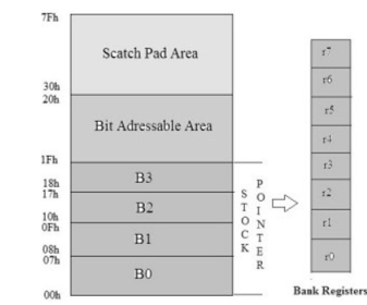
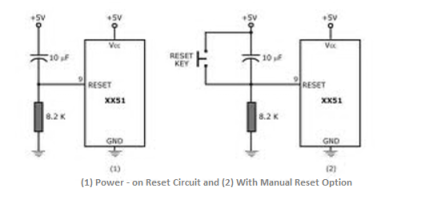
Figure. General Purpose MemoryThe general-purpose memory is called as the RAM of the 8051 microcontrollers, which is divided into 3 areas such as banks, bit-addressable area, and scratch-pad area. The banks contain different general-purpose registers such as R0-R7, and all such registers are byte-addressable registers that store or remove only 1-byte of data.Q5) Explain clock and reset circuits?A5)RESET is an active High input. When RESET is set to High, 8051 goes back to the power on state. The 8051 is reset by holding the RST high for at least two machine cycles and then returning it low.There are two method of reset circuit: 1.Power on Reset. Initially charging of capacitor makes RST High When capacitor charges fully it blocks DC. 2.Manual Reset Closing the switch momentarily will make RST High.
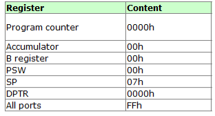
Figure . Power and Reset Circuit After a reset, the program counter is loaded with 0000H but the content of on-chip RAM is not affected.
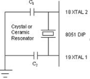
OSCILLATOR CIRCUIT OF 8051 CONTROLLERThe 8051 uses the crystal for precisely that to synchronize it’s operation. Effectively, the 8051 operates called as "machine cycles." A single machine cycle is the minimum amount of time in which a single 8051 instruction can be executed. although many instructions take multiple cycles. 8051 has an on-chip oscillator. It needs an external crystal that decides the operating frequency of the 8051.
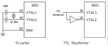
Figure. Oscillator circuit This can be achieved in two ways.The crystal is connected to pins 18 and 19 with stabilizing capacitors. 12 MHz (11.059MHz) crystal is often used and the capacitance ranges from 20pF to 40pF. The oscillator can also be a TTL clock source connected with a NOT gate as shown.
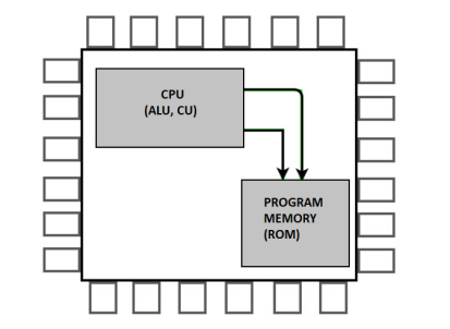
Figure. Crystal Oscillator Circuit Q6) Explain Program Memory?A6)The code or instructions which are to be executed are stored in the Program Memory, also called as the ROM of the Microcontroller.
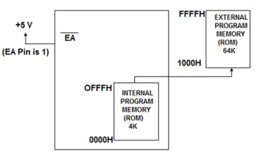
Figure 7. Program MemoryIn 4KB Internal ROM, the address space is 0000H to 0FFFH. If the program addresses exceed this value,CPU will automatically fetch the code from the external Program Memory.For External Access (EA Pin) must be pulled HIGH at this condition the CPU first fetches instructions from the Internal Program Memory in the address range of 0000H to 0FFFFH .If it exceeds the memory addresses limit, instructions are fetched from external ROM in address range of 1000H to FFFFH.
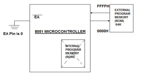
Figure 8. External access There is also an alternative method to fetch the instructions where the Internal ROM is ignored and instructions are fetched only from External Program Memory(External ROM).For this purpose, EA pin must be connected to GND. The memory addresses of external ROM will be from 0000H to FFFFH.
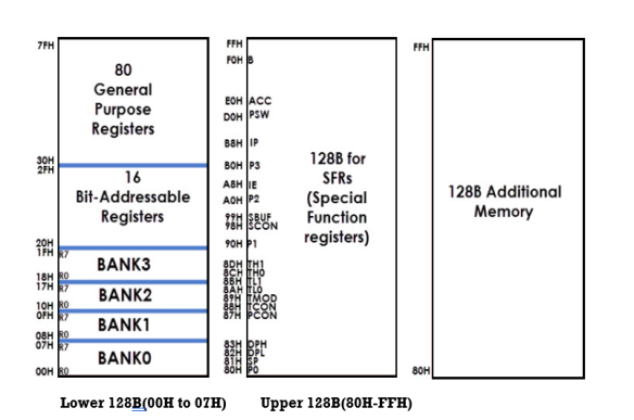
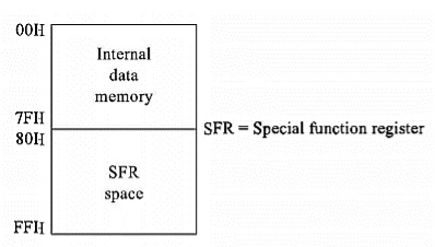
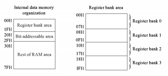
Figure. External Program Memory Q7) Explain Data Memory?A7) Data Memory or RAM stores temporary data and intermediate results generated during the normal operation of the microcontroller. Currently, 8051 Microcontroller has 256B of RAM. The first 128B memory addresses from 00H to 7FH is divided in to Working Registers. They are organized as Register Banks, Bit – Addressable Area and General Purpose RAM known as Scratchpad area. The first 128B of RAM (from 00H to 7FH), the first 32B of memory from addresses 00H to 1FH consists of 32 Working Registers organized into four banks with 8 Registers in each Bank.
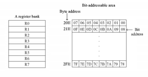
Lower 128B(00H to 07H) Upper 128B(80H-FFH)(Direct and Indirect Addressing) (Direct Addressing) (Indirect Addressing) The 4 banks are named as Bank0, Bank1, Bank2 and Bank3. Each Bank consists of 8 registers R0 – R7. Each Register can be addressed either by name or by address. To address the register by name, first the corresponding bank is selected. In order to select the bank, RS0 and RS1 bits of the Program Status Word (PSW) and Register (RS0 and RS1 are 3rd and 4th bits in the PSW Register) are used. When addressing these Register for example 12H the corresponding bank may or may not be selected. (12H corresponds to R2 in Bank2). The next 16B of the RAM that is from 20H to 2FH are Bit – Addressable memory locations. A total of 128 bits can be addressed individually using 00H to 7FH or an entire byte can be addressed as 20H to 2FH. The final 80B of the internal RAM addresses are from 30H to 7FH which is the general-purpose RAM area are byte addressable. These lower 128B of RAM can be addressed directly or indirectly. Q8) Write a short note on timing and execution cycles?A8) The cycle starts immediately when power is applied to the system using initial PC value A cycle includes:Instruction Fetch Instruction Decode Data Fetch/ Operand Fetch Instruction Execution Result Return. Fetch:The CPU sends PC to Memory Address Register. The CPU activates tri-state buffer so MAR contents are placed on the address bus. CPU activates tri-state buffer so MAR contents are placed on the address bus. CPU sends read command on the control bus,R/W =1 and CE =1 to memory to indicate that it wants to read. In response to read command the memory returns the data stored in the memory location. Decode Instruction The decoding process allows the CPU to determine what instruction be performed so that CPU can tell how many operands it needs to fetch in order to perform the instruction. The opcode fetched from memory is decoded for next step to be moved into appropriate registers. Execute the Instruction If arithmetic or logic instruction is used utilize the ALU circuits to carry out the operation on data in registers. This is the only stage of the instruction cycle from the end user perspective. Storing the Result If destination is a memory address initiate memory write cycle to transfer the result from CPU to memory. Q9) Write a short note on Register Bank?A9)8051 Provides four register bank, but only one register bank can be used at any point in time. To select the register bank, two bits of PSW (Program Status Word) are used.
|
Addition, subtraction with carry, and multiplication come under arithmetic operations.
Logical AND, OR and exclusive OR (XOR) come under logical operations.
Q3) Explain address, data and control bus?A3)Basically, Bus is a collection of wires which work as a communication channel or medium for transfer of Data. There are three internal buses associated with processors: the data bus, address bus, and control bus. Together, these three make up the “system bus.”
|
|
|
|
|
|
|
|
|
Address Range | Register Bank |
00H to 07H | Register Bank 0 |
08H to 0FH | Register Bank 1 |
10H to 17H | Register Bank 2 |
18H to 1FH | Register Bank 3 |
8051 Provides four register bank, but only one register bank can be used at any point in time. To select the register bank, two bits of PSW (Program Status Word) are used.
Figure . Register Bank So, the following addressing can be used to select register banks.The concept of four register banks is very useful. For servicing the interrupts, this feature is good. The interrupt program can use one bank, and the interrupt Service Subroutine (ISS) can access another bank for better performance. As there are four banks, so for nested interrupts these can be used Q10) Explain Internal Data Memory Organization?A10)
When all of the register banks are being used, the scratch pad area will be 20H to 7FH. But from 20H to 2FH (16 bytes or 128 bits) can be used as bit addressable RAM. Another section of bit addressable locations is 80H to FFH. The remaining locations (30H to 7EH) of the RAM can be used to store variable data and stack.
|
|
|
0 matching results found
