Unit - 3
SEQUENTIAL CIRCUIT DESIGN
Q1) Define Pipelining
A2) Pipelining is a popular design technique often used to accelerate the operation of the data path in digital processors. The major advantages of pipelining are to reduce glitching in complex logic networks and getting lower energy due to operand isolation.
Q2) Compare & Contrast synchronous design and asynchronous design
A2) Synchronous Sequential Circuit: Output changes at discrete interval of time. It is a circuit based on an equal state time or a state time defined by external means such as clock. Examples of synchronous sequential circuit are Flip Flops, Synchronous Counter.
Asynchronous Sequential Circuit: Output can be changed at any instant of time by changing the input. It is a circuit whose state time depends solely upon the internal logic circuit delays. Example of asynchronous sequential circuit is Asynchronous Counter
Q3) Define clock skew and clock jitter
A3) Clock skew: In reality clocks have some uncertainty in their arrival times that can cut into the time available for useful computation is called clock skew
Clock jitter: Temporal variations in consecutive edges of the clock signals; modulation + random noise- Cycle-to-cycle (short-term) long term
Q4) List out the techniques used for low power logic design
A4)
To reduce the dynamic power, supply voltage VDD is reduced.
The transistors with minimum size can be used to reduce the capacitances.
The power dissipation due to short circuit current is minimized by matching the rise time/fall times of the input and output signals.
Proper layout techniques are used to minimize routing capacitances.
Q5) Difference between latch and flip-flop
A5)
S.No | Latch | Flip-Flop |
1 | A Latch is Level-Sensitive | A Latch stores when the clock level is low and is transparent when the level is high |
2 | A FF is edge triggered | A FF stores when the clock rises and is mostly never transparent |
Q6) List out the techniques used for low power logic design
A6)
To reduce the dynamic power, supply voltage VDD is reduced
The transistors with minimum size can be used to reduce the capacitances.
The power dissipation due to short circuit current is minimized by matching the rise time/fall times of the input and output signals.
Proper layout techniques are used to minimize routing capacitances.
Q7) What is clocked CMOS registers
A7) The dynamic latch can also be drawn as a clocked tristate. Such a form is sometimes called clocked CMOS (C2MOS) the output is driven through the nMOS and pMOS working in parallel. C2MOS is slightly smaller because it eliminates two contacts.
Q8) Explain the methodology of sequential circuit design of latches and flip-flops
A8) The Bistability Principle:
Static memories use positive feedback to create a bistable circuit — a circuit having two stable states that represent 0 and 1.

Fig. Bistability
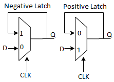
Multiplexer Based Latches
Multiplexer based latches can provide similar functionality to the SR latch, but has the important added advantage that the sizing of devices only affects performance and is not critical to the functionality.
Positive latch: When CLK=0 D input is passed to output, when CLK=1 input 1 is connected to output of latch.
Negative latch: When CLK=0 output is feedback to input, when CLK=1 input 1 D is selected.

Fig. Multiplexer based latches
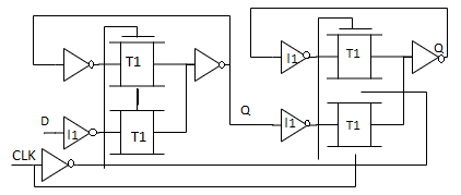
Master-Slave Based Edge Triggered Register:
When clock is low (CLK = 1), T1 is on and T2 is off, and the D input is sampled onto node QM.
When the clock goes high, the master stage stops sampling the input and goes into a hold mode.

Fig. Master slave edge triggered register
Q9) Draw and explain the operation of Conventional latches
A9) Conventional latches:

The conventional form using the inverter and transmission gate is slightly faster because the output is driven through the nMOS and pMOS working in parallel. When the clock is 1, the input transmission gate is ON, the feedback tristate is OFF, and the latch is transparent. When the clock is 0, the input transmission gate turns OFF. However, the feedback tristate turns ON, holding X at the correct level.
Q10) Explain clock distribution techniques in synchronous design in detail
A10)
