Unit - 5
IMPLEMENTATION STRATEGIES AND TESTING
Q1) Discuss the details about speed and area trade off
A1) Speed, area and power can be trade off through the choice of the supply voltages, transistor threshold and device sizes. Some design techniques are implemented at design time. Transistor width s and lengths can be fixed at the time of design. A reduction in supply voltage results in power savings and thus is the most attractive approach. Reduced supply evenly lowers the power dissipation of all the logic gates. In this approach, non –critical path having timing slack is supplied with low voltage without affecting the system performance.
Important design concepts: - To select right structure before starting an circuit optimization. - Determine the critical timing path through the circuit. - Circuit size is not only determined by the number and size of the transistors. - An obscure optimization can sometimes help to get a better result. - Power and speed can be traded off through a choice of circuit sizing, supply voltages and transistor threshold
Q2) Name the elements in a Configurable Logic Block
A2) Feed through is a piece of metal used to pass a signal through a cell or to a piece in a cell. The connection between the rows of standard cell is made by feed through.
Q3) Write the various ways of routing procedures
A3) Global routing architecture Detailed routing architecture FPGA interconnect routing.
Q4) What is an antifuse? State its merits and demerits.
A4) An antifuse is normally high resistance (>100MΩ). on application of appropriate programming voltages, the antifuse is changed permanently to a low-resistance structure(200-500Ω).
Q5) Differentiate between channelled and channel less gate array.
A5)
S.No | Channelled Gate Array | Channel less Gate Array |
1 | Only the inter corner is customized | Only the top few mask layers are customized |
2 | The interconnect user predefined spaces between rows of base cells | No predefined areas are set aside for routing between cells. |
3 | Routing is done using the spaces | Routing is done using the area of transistors |
4 | Logic density is less | Logic density is higher |
Q6) Discuss different types of programming technology used in FPGA design
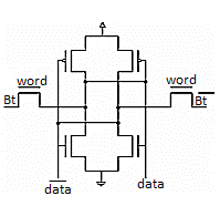
A6) SRAM-Based Programming Technology
Static memory cells are the basic cells used for SRAM-based FPGAs.
In an SRAM-based FPGA, SRAM cells are mainly used for following purposes: - To program the routing interconnect of FPGAs which are generally steered by small multiplexors. - To program Configurable Logic Blocks (CLBs) that is used to implement logic functions. - Further SRAM cells are volatile in nature and external devices are required too permanently.
Flash Programming Technology
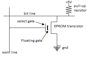
Flash-based programming technology offers several advantages. Flash-based programming technology is also more area efficient than SRAM-based programming technology. Flash-based programming technology has its own disadvantages also. Unlike SRAM-based programming technology, flash -based devices cannot be reconfigured/reprogrammed an infinite number of times. Also, flash-based technology uses non-standard CMOS process.
Q7) Explain FPGA building block architecture?
A7) The field-programmable gate array (FPGA) is an integrated circuit that consists of internal hardware blocks with user-programmable interconnects to customize operation for a specific application.
FPGA architecture consists of thousands of fundamental elements called configurable logic blocks (CLBs) surrounded by a system of programmable interconnects, called a fabric, that routes signals between CLBs. Input/output (I/O) blocks interface between the FPGA and external devices.
Depending on the manufacturer, the CLB may also be referred to as a logic block (LB), a logic element (LE) or a logic cell (LC).
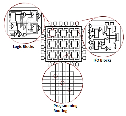
Fig: FPGA architecture
An individual CLB is made up of several logic blocks. A lookup table (LUT) is a characteristic feature of an FPGA. An LUT stores a predefined list of logic outputs for any combination of inputs: LUTs with four to six input bits are widely used. Standard logic functions such as multiplexers (mux), full adders (FAs) and flip-flops are also common.
The number and arrangement of components in the CLB varies by device.
It contains two three-input LUTs an FA and a D-type flip-flop plus a standard mux and two muxes, that are configured during FPGA programming.
This simplified CLB has two modes of operation. In normal mode, the LUTs are combined with Mux 2 to form a four-input LUT; in arithmetic mode, the LUT outputs are fed as inputs to the FA together with a carry input from another CLB.
Current-generation FPGAs include more complex CLBs capable of multiple operations with a single block; CLBs can combine for more complex operations such as multipliers, registers, counters and even digital signal processing (DSP) functions.
Q8) Explain the types of FPGA interconnect routing?
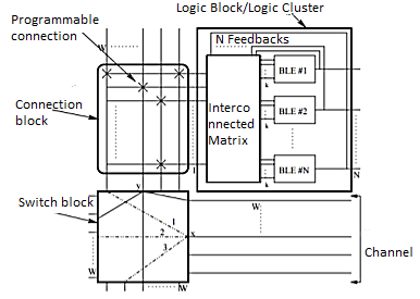
A8) Global routing
Detail routing
Q9) Explain ad hoc testing?
A9) ad hoc testing combines a collection of tricks and techniques that can be used to increase the observability and controllability of a design and that are generally applied in an application-dependent fashion. An example of such a technique is illustrated in Fig. (a), which shows a simple processor with its data memory. Under normal configuration, the memory is only accessible through the Processor. Writing and reading a data value into and out of a single memory position requires a number of clock cycles.
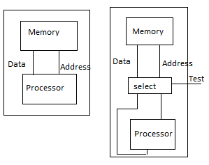
The controllability and observability of the memory can be dramatically improved by add multiplexers on the data and address buses (Fig.). During normal operation mode, these selectors direct the memory ports to the processor. During test, the data and address ports are connected directly to the I/O pins, and testing the memory can proceed more efficiently. The example illustrates some important design-for testability concepts.
It is often worthwhile to introduce extra hardware that has no functionality except improving the testability. Designers are often willing to incur a small penalty in area and performance if it makes the design substantially more observable or controllable. Design-for-testability often means that extra I/O pins must be provided besides die nominal functional I/O pins. The test port in Fig.(b) is such an extra pin. To reduce the number of extra pads that would be required, one can multiplex test signals and functional signals on the same pads. For example, the I/O bus in Fig. (b) serves as a data bus during normal operation and provides and collects the test patterns during testing.
An extensive collection of ad hoc test approaches has been devised. Examples include the partitioning of large state machines, addition of extra test points, prevision of reset states, and introduction of test buses. While very effective, the applicability of most of these techniques depends upon the application and architecture at hand. The insertion into a given Hating requires expert knowledge and is difficult to automate. Stricture and automatable approaches are more desirable.
Q10) Explain the Scan design procedure?
A10) Scan Design Rules