AC
Unit-5Power Amplifiers Q1) Explain power dissipation in transistor?A1) When a transistor conducts current between collector and emitter, it also drops voltage between those two points. At any given time, the power dissipated by a transistor is equal to the product of collector current and collector-emitter voltage. Just like resistors, transistors are rated for how many watts each can safely dissipate without sustaining damage.High temperature is the mortal enemy of all semiconductor devices, and bipolar transistors tend to be more susceptible to thermal damage than most. Power ratings are always referenced to the temperature of ambient (surrounding) air. When transistors are to be used in hotter environments >25o, their power ratings must be derated to avoid a shortened service life. Q2) Explain Class A amplifiers?A2) A class-A amplifier is the amplifier in which the Q-point of the input signal are selected such that the output signal is obtained for a full input cycle. For this purpose, the position of the Q-point is approximately at the midpoint of the load line. For all the values of the input signal, the transistor remains in the active region and never enters into cut-off or saturation region.
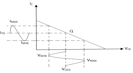
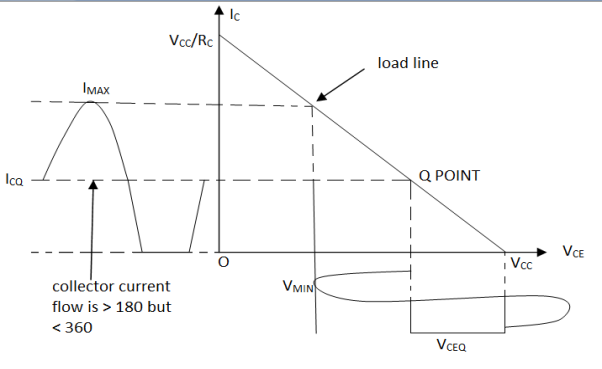
Fig 1 Output characteristics of CE AmplifierThe collector current IC flow for complete 3600 (full cycle) of the input cycle. Thus, the angle of the collector current flow is 3600. Class A amplifier are of 2 types –( i ) Directly coupled class A amplifier – In directly coupled type, the load is directly connected in the collector circuit. ( ii ) Transformer coupled class A amplifier – In this the load is coupled to the collector using a transformer called an output transformer.( i ) Directly coupled class A amplifier –
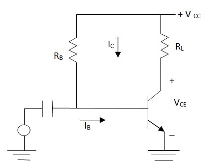
Fig 2 Directly coupled class A amplifierThe value of RB is selected such that Q point lies at the centre of d.c. load line.VCC = ICRL + VCE IBQ = VCC – 0.7 / RBICQ = βIBQVCEQ = VCC - ICQRLDC power input : PDC = VCCICQ WattsThe d.c. power input is provided by the supply :With no a.c. input signal, the d.c. current drawn is the collector bias current ICQ. Even if any a.c. input signal is applied, the average current drawn from the d.c. supply remains same. A.C. power Output : Vpp = Vmax - VminVmin = Min instantaneous value of collector output voltageVmax = Max instantaneous value of collector output voltageVpp = Peak of a.c. output voltage Vm = Vpp / 2 = Vmax – Vmin / 2 = Amplitude of a.c. output voltageIm = Ipp / 2 = Imax – Imin / 2The r.m.s value of alternating output voltage and current is given as Vrms = Vm / √2 ; Irms = Im / √2Pac = VrmsIrms = I2rmsRL = V2rms / RLPac = Vm /√ 2 : Im /√ 2 = 1/2Vmax – Vmin /√ 2 . Imax – Imin /√ 2Pac = ( Vmax - Vmin )( Imax - Imin ) / 8Efficiency: % n = Pac / Pdc x 100 % = [(Vmax - Vmin) (Imax - Imin) / 8 x Vcc x ICQ] x 100%
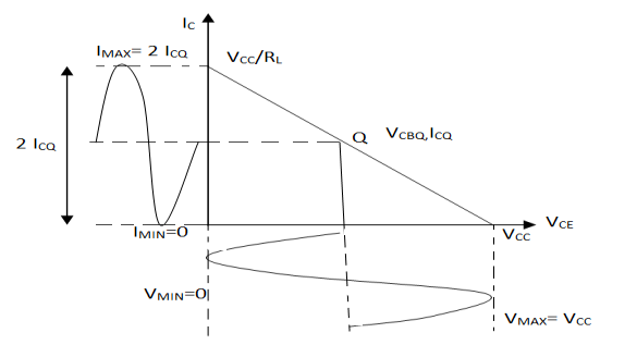
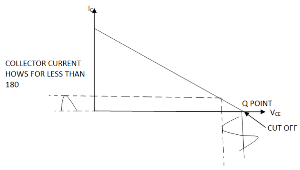
Fig 3 AC Power OutputMaximum Efficiency: Vmax = Vcc, Vmin = 0Imax = 2ICQ, Imin = 0 { As Q is in middle }n = (Vmax - Vmin) (Imax - Imin) / 8 x Vcc. ICQ x 100 % = (Vcc - 0)(2ICQ - 0) / 8 x Vcc.ICQ x 100 %Nmax = 25 % { Biggest disadvantage } Q3) For class A amplifier explain power dissipation and disadvantages?A3) Power dissipation = D.C. power input – AC power output( i ) When there is no input signal, then Pac = 0 and the entire d.c power gets dissipated in the form of heat which is maximum PD. (Pd)max = PDC = VCCICQ when Pac = 0( ii ) When input signal is larger, more power is delivered to load ( Pac is more ) and less is the power dissipation. Thus class A amplifier dissipated less power when delivers maximum power to the load while it dissipates maximum power while delivering zero power to the load. Disadvantages:( i ) The load resistance is connected directly to collector, hence quiescent current passes through this resistance. This current represents a considerable waste of power, since it doesn’t contribute to the a.c. component of the power. Also it is inadvisable to pass the d.c. component of current through the output device. ( ii ) Efficiency is poor. Q4) Explain class B amplifiers?A4) In class B amplifiers, the Q point and the input signal is selected, such that the output signal is obtained only for one half cycle for a full input cycle.Either the quiescent current or the quiescent voltage is approximately zero. If quiescent current is zero, then the transistor is in cut off region, and the transistor remains in active region only for the half cycle of the input signal. Hence at output we get only the half cycle.
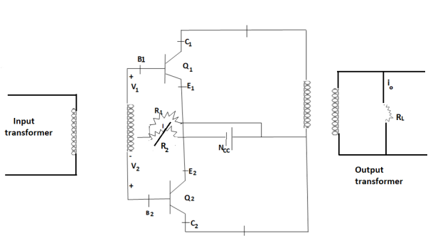
Fig 5 Load line characteristics of class B amplifierIf instead of ICQ = 0, we would have taken VCEQ = 0( i.e. Q point on Y-axis ) then the transistor would have been in saturation region and the collector current flows only for negative half cycle of the input signal. Efficiency of this mode is higher than class A mode. Since in this mode, collector current flows only for half cycle, so that output signal is distorted. To get the full cycle, a pair of transistors is used in class B operation. The 2 transistors conduct in alternate half cycles of the input signal abd so a full cycle across the load is obtained. The two transistors are identical in characteristics and are called matched transistors. Q5) Explain push pull class B amplifiers?A5)When both the transistors are of some type i.e. either n-p-n or p-n-p, then the circuit is called push-pull class B audio frequency power amplifier.The push pull circuit requires 2 transformers, one as input transformer called driver transformer and the other to connect the load called output transformer. The input signal is applied to the primary of the driver transformer. Both the transformer are centre tapped transformers.
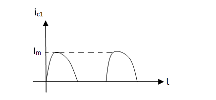
Fig 6 Push pull amplifierIn the circuit, both Q1 and Q2 are of n-p-n type. p-n-p can also be used but with -VCC. Both are in CE configuration.Operation:Case ( i ) – During positive half cycle,Q1 = ON, Q2 = OFFIO1α iC1
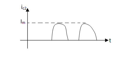
Fig 7 Positive half cycle output Case ( ii ) – During negative half cycle,Q1 = OFF, Q2 = ONIO2α iC2
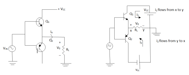
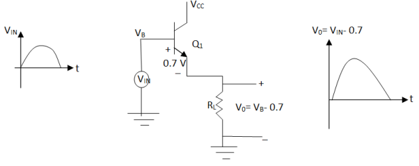
Fig 8 Positive half cycle output Case ( iii ) When signal is absent i.e. V1 = V2 = 0If R2 = 0 then,VBE1 = VBE2 = 0Both Q1, Q2 are in cut off [ Class B operation] Case ( iv ) If R2 increases then IR2 increases and when IR2 = Vr thenVBE1 = VBE2 = Vr [ Class AB operation] Case ( v ) If R2 increases more, then IR2 increases VBE increases and Q point will move towards saturation.The total d.c. power is given by,Pdc = VCC x Idc = 2 / ∏ VCC Ima.c. power, Pac = Vrms.Irms = I2rmsR1L = V2rms / R1LEfficiency:% n = Pac / Pdc x 100 % = ( Vm.Im / 2 ) / 2 / ∏VCCIm% n = ∏ / 4 Vm / VCC x 100 % Max Efficiency:Max efficiency is possible only if, Vm = VCC% nmax = ∏ / 4 VCC / Vcc x 100 = 78.5 % Power dissipation: Pd = Pdc - Pac= 2 / ∏ VCCIm - Vm.Im / 2= 2 / ∏ VCCVm/ R1L - Vm2 / 2 R1LMaximum power dissipation:For max power dissipation,dPd / dVm = 2 / ∏ VCC / R1L - 2Vm/ 2 R1L = 02 / ∏ VCC / R1L = Vm/ R1L Vm = 2 / ∏ VCCThis is the condition for max power dissipation,Hence max power dissipation is given by,(Pd)max = 2 / ∏ VCC x 2 / ∏ VCC / R1L - 4 / ∏2 VCC2 / 2R1L = 4 / ∏2 VCC2 / R1L - 2 / ∏2 VCC2 / R1L(Pd)max = 2 / ∏2 VCC2 / R1L Q6) Explain complimentary symmetry class B push pull amplifier?A6) This circuit is transformer less circuit. But with common emitter configuration, it becomes difficult to match the output impedance for maximum power transfer with output transformer. Hence the matched pair of complementary transistors is used in common collector (emitter follower) configuration in this circuit.This is because common collector configuration has lowest output impedance and hence the impedance matching is possible.
Fig 9 Complimentary symmetry Push pull amplifierThe circuit is driven from a dual supply of +-VCC. The transistor Q1 is n-p-n while Q2 is p-n-p type. Operation:During positive half cycle:
Fig 10 Positive half cycle operationDuring negative half cycle:
Fig 11 Negative half cycle operation Cross over distortion:
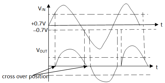
Fig 13 Crossover Distortion Q7) Explain class AB amplifiers?A7) In class AB amplifiers, the Q-point and the input signal are selected such that the output signal is obtained for more than a half cycle but less than a full cycle.
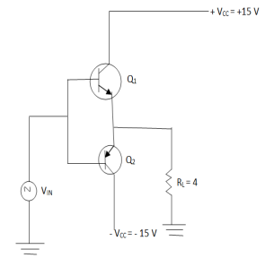
Fig 14 Characteristic curve for class AB operationThe Q point is below the midpoint but above X-axis or above the midpoint but to the right of Y-axis. Its efficiency is more than class A but less than class B. Efficiency increases as the Q-point moves away from the centre of the load lineQ8) Determine the input power, output power and efficiency resulting in a class B push-pull amplifier providing a signal 20V peak to a 16 Ω load, using a single supply of VCC = 30V.A8) Given: VL(p) = 20 V, RL = 16 Ω, VCC = 30 V The input power is given by,Pi(dc) = VCC(2 / ∏ I / p) = VCC.2 / ∏.VL(p) / RL = 30 x 2 / ∏ x 20 / 16 = 23.87 W Ans.The output power is given by, PO(ac) = VL2(p) / 2RL = VL2(rms) / 2RL = (20)2 / 2 x 16 = 12.5 W Ans.Thus efficiency is given by,n = PO(ac) / Pi(dc) x 100 = 12.5 / 23.87 x 100 = 52.37 % Ans. Q9) Class B complementary A.F. power amplifier shown in the below figure
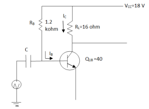
Calculate:Maximum a.c. power which can be developed. Collector dissipation while developing maximum a.c. power. Efficiency Maximum power dissipation per transistor. Efficiency under maximum power dissipation condition Assume sinusoidal input. A9) Given: VC = 15 V, RL = 4 ΩUse the expression derived for push pull class B.The maximum a.c. power is, (Pac)max = 1/2VCC2 / RL = 1/2(15)2 / 4 = 28.125 W AnsWhen power developed is maximum, Vm = VCC RL = Vm / ImIm = Vm / RL = VCC / RL = 15 / 4 = 3.75 APdc = 2 / ∏VCCIm = 2 / ∏ x 1.5 x 3.75 = 35.809 WPd = Pdc – Pac = 35.809 – 28.125 = 7.684 W Ans.This is the total collector dissipation under maximum power conditions. Efficiency: % n = Pac / Pdc x 100 = 28.125 / 38.809 x 100 = 78.5 % Ans.The efficiency is maximum possible for class B, due to the fact that the power developed is at its maximum.For maximum power dissipation, Vm = 2 / ∏ VCC = 2 / ∏ x 15 = 9.5492 V Im = Vm / RL = 9.5492 / 4 = 2.3873 APdc = 2 / ∏ VCC Im = 2 / ∏ x 15 x 2.3873 = 22.797 WWhile Pac = 1/2Vm2 / RL = 1/2(9.5492)2 / 4 = 11.398 W(Pd)max = Pdc – Pac = 22.797 – 11.398 = 11.39 W(Pd)max = 11.39 / 2 = 5.699 W [ Per transistor]Alternatively, we can directly use the result,(Pd)max = 2 / ∏2 (Pac)max per transistor = 2 / ∏2 x 28.125 = 5.699 W per transistor Ans.Efficiency under (Pd)max condition, % n = Pac under (Pd)max / Pdc under (Pd)max x 100 = 11.398 / 22.797 x 100 = 50 % Ans. This shows that when efficiency is maximum, power dissipation is not maximum and when power dissipation is maximum, efficiency is not maximum. Q10) A series fed class A amplifier uses a supply voltage of 10 V and load resistance of 20 Ω. The a.c. input voltage results in a base current of 4 mA peak. Calculate,D.C. input power A.C. output power % efficiency Assume β of the transistor as 25 and the collector bias current of 50 mA.(B) Calculate the input power, output power & the efficiency of class A amplifier shown in figure. The input voltage causes a base current 5mA rms.
A10)(A) Given: VCC = 10 V, (ib)m = 4 mA, β = 25, ICQ = 50 mA, RL = 20 ΩD.C. input power: PDC = VCCICQ = 10 x 50 x 10-3 = 0.5 W Ans.A.C. output power: (ic)m = β(ib)m = 25 x 4 = 100 mA But ic is the output current I.Im = 100 mAPac = I2mRL / 2 = (100 x 10-3)2 x 20 / 2 = 0.1 W Ans.% Efficiency: % n = Pac / Pdc x 100 = 0.1 / 0.5 x 100 = 20 % Ans (B) Given class A amplifier is shown in below figure
Current IBQ can be written as,IBQ = VCC – 0.7 / RB = 18 – 0.7 / 1.2 x 103 = 14.4167 mANow, ICQ = βIBQ = 40 x 14.4167 = 576.67 mAAnd, VCEQ = VCC – ICQ RL = 18 – 576.67 x 10-7 x 16 = 8.7733 VSo, Pdc = VCCICQ = 18 x 576.67 = 10.38 W Ans.This is the input power.(Ib)rms = 5 mA(Ic)rms = β(Ib)rms = 40 x 5 = 200 mAThis is nothing but the output collector current r.m.s value Irms.Irms = 200 mAOutput power can be written as,Pac = I2rms RL = (200 x 10-3) x 16 = 640 mWThis is the power delivered to the load.Hence the efficiency of the amplifier is,% n = Pac / Pdc x 100 = 640 x 10-3 / 10.38 x 100% n = 6.165 % Ans.
|
|
|
|
|
|
|
|
|
|
|
|
|
|
|
0 matching results found
