|
|
|
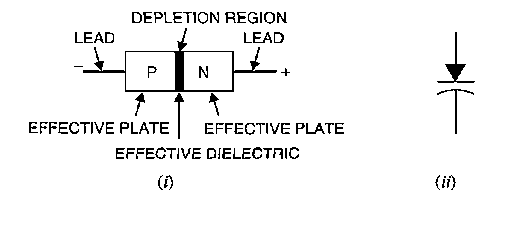
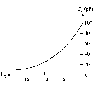
 Where CT = Total capacitance of the junction Ɛ = Permittivity of the semiconductor material A = Cross-sectional area of the junction Wd= Width of the depletion layer When reverse voltage across a varactor diode is increased, the width Wd of the depletion layer increases. Therefore, the total junction capacitance CT of the junction decreases. On the other hand, if the reverse voltage across the diode is decreased, the width Wd of the depletion layer decreases. Consequently, the total junction capacitance CT increases.
|
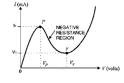
 Figure: Symbol of tunnel diode We can also define it as “A tunnel diode is a pn junction that exhibits negative resistance between two values of forward voltage (i.e., between peak-point voltage and valley-point voltage)”. We know that a conventional diode exhibits "positive resistance when it is forward biased or reverse biased but this is not happening in tunnel diode.The tunnel diode is basically a pn junction with heavy doping of p-type and n-type semiconductor materials. Doping in a tunnel diode is approximately 1000 times as heavily as a conventional diode. This heavy doping results in a large number of majority carriers. Because of the large number of carriers, most are not used during the initial recombination that produces the depletion layer. As a result, the depletion layer is very narrow. In comparison with conventional diode, the depletion layer of a tunnel diode is 100 times narrower. Working of tunnel diode includes the quantum tunneling effect and that’s why it is named as tunnel diode. Let us recall the tunnelling effect. Tunneling effect: There are large numbers of majority carriers because of the heavy doping. These carriers drift in p and n sections.Many valence electrons raised their energy level closer to the conduction region because of the drift activity. The movement of valence electrons from the valence energy band to the conduction band with little or no applied forward voltage is called tunneling. Valence electrons seem to tunnel through the forbidden energy band. As we increase the forward voltage, current in the diode rises initially due to tunneling effect. But on further increasing of forward voltage the tunneling effect is reduced and current flow starts to decrease. Thus tunnel diode is said to have entered the negative resistance region. As the voltage is further increased the tunneling effect plays less and less part until a valley-point is reached. From now onwards, the tunnel diode behaves as ordinary diode i.e., diode current increases with the increase in forward voltage. V-I Characteristic
|
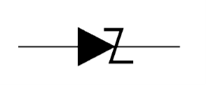 Figure: Symbol of a zener diode
|
|
|
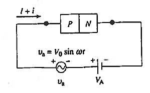
Figure : Diode biasing circuit
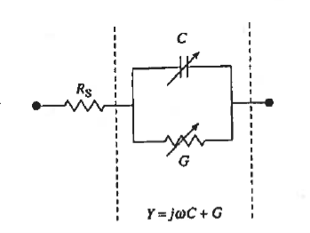
Figure : Equivalent pn diode circuit
|
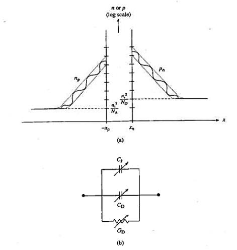
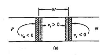
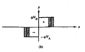
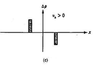
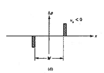
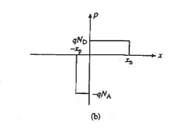
 charge density oscillation, as pictured in Figure 28(c) and (d). The p-plots were obtained by subtracting the d.c. charge density distribution in Fig. 7.4(b) from the VA ± va charge density distribution.The diode capacitance is concluded
  The capacitance associated with the depletion width oscillation is known as the junction or depletion-layer capacitance
|
|
 ………(1)The value of M can be obtained from experimental fact as
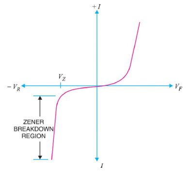
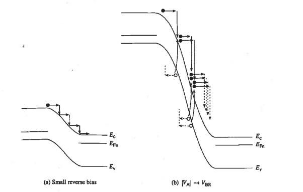
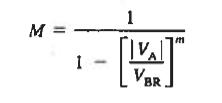 ………(2)where power in the denominator m can have value between 3 and 6. m depends upon the type of semiconductor used in manufacturing the diode. We next seek to explain the Veit dependence noted in the breakdown introduction. From the qualitative description of avalanching, it was concluded that Breakdown occurs when the carriers gain an ionizing amount of energy in traveling a lattice-scattering mean free path. This should be true independent of the junction doping. A specific energy gain over a given distance, however, corresponds to a specific electric field. In other word.. breakdown occurs when the electric field in the depletion region reaches some critical value ξCR. essentially independent of the junction doping. Considering a step junction, evaluating the electric field at x = 0, we find
|
 ………(4)Since ξCR is independent of doping, the right-hand side of Eq. (4) must likewise be independent of doping. The right-hand side of Eq. (4) will be independent of doping if
  ………(5)or for asymmetrically doped junctions
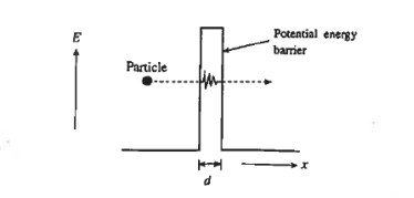
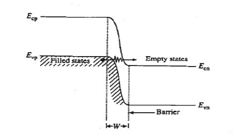
 ………(6)The Eq. (6) is close enough to the experimental result. VBR increases with increase in temperature.Lattice scattering increases with increase in temperature, Lattice scattering increases means a smaller mean free path, a larger critical electric field for avalanching, and hence a higher breakdown voltage. Q 9) Explain zener process? A 9)Zener Process is tunneling in a reverse-biased diode.We already know that tunneling is quantum phenomena it does not have any classical analogy. As you can see in figure the tunnelling. Particle is travelling from left to right face a potential barrier. The height of the barrier is assumed to be greater than the kinetic energy of the particle. Classically, the particle can cross this barrier after getting sufficient energy and go over the top of the barrier. However, Quantum mechanically, there is another way the particle can cross the barrier. The process of particle moving through the potential barrier is known as Tunneling. The particle energy remains constant during the process. Requirements for tunnelling to occur are given below: (I) There must be filled states on one side of the barrier and empty states on the other side of the barrier at the same energy. Tunneling cannot take place into a region void of allowed states. (2) The width of the potential energy barrier, d must be very thin. Quantum-mechanical tunneling becomes significant only if d < 100 Å = 10-6 cm.
|
|
 ……….(1)
|
 |thermal R-G =-
 n is not applicable. Rather, the general-case result is applied
|
 then integral in Eq. (3) becomes
Where
………..(5)
|
 kT), 1<
 2, for forward biases greater than a few kT/q. Typically, the expected
  is close to 2, and the combined forward and reverse bias dependence is approximately described by
|
|
 …………(8) We concluded that
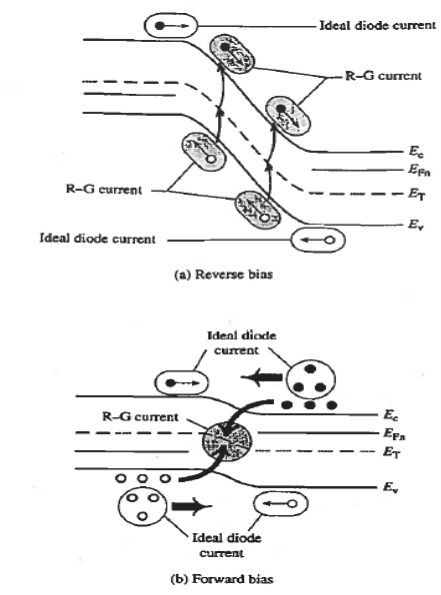
  0 and the IR-G current dominates at reverse biases and small forward biases.
  kT) for VA > kT/q,
  while IR-G
  the relative weight of the two components varies significantly from semiconductor to semiconductor.
|
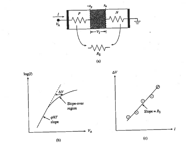
 V voltage displacement between the two curves as a function of I Since
  V =VJ - VA= IRs , the slope of the line through a plot of the
  V versus I data yields Rs.
|
 V versus I (c)
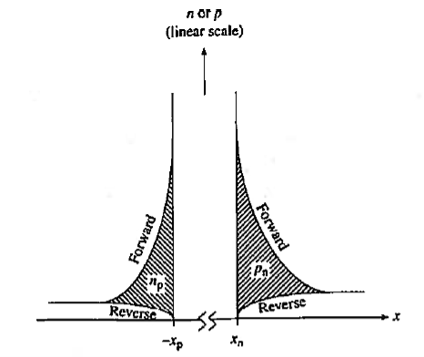
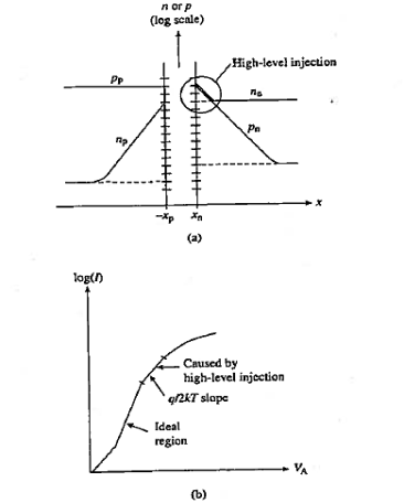
  V versus / plot used to deduce Rs. Q 12) Explain high-level injection? A 12)HIGH-LEVEL INJECTIONTo derive ideal diode equation, we made the assumption of low-level injection but unfortunately it fail when the minority carrier concentration at the depletion region edge on the lightly doped side of the junction approaches the doping concentration. In Si at room temperature this typically occurs at applied voltages a few tenths of a volt below Vbi . A further increase in the applied voltage gives rise to high-level injection. Under high-level injection both the minority carrier and the majority carrier concentrations adjacent to the depletion region are perturbed, as shown in Figure 22 (a).
|
|
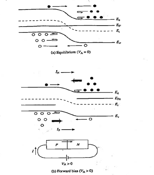
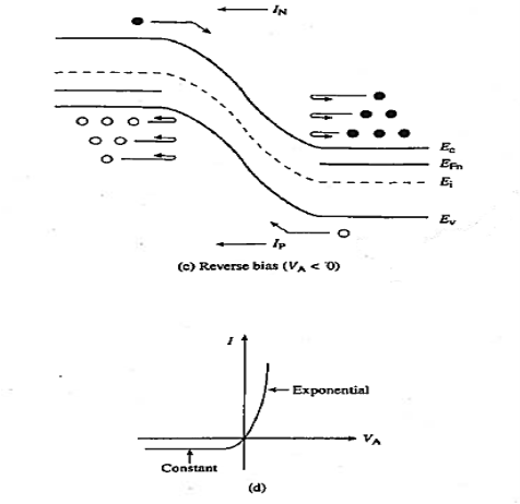
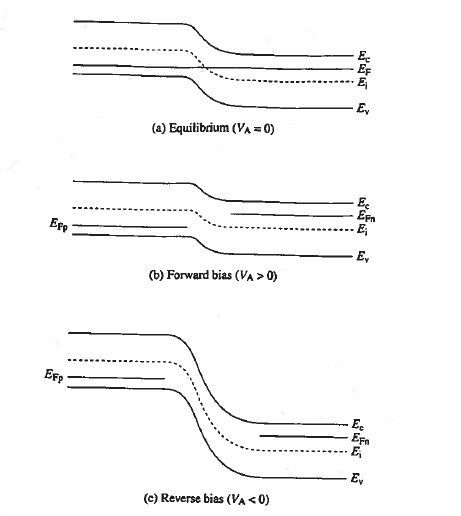
Figure 15: pn junction energy band diagram, carrier distribution, and carrier activity near the depletion region (a) equilibrium (VA = 0), (b) forward bias, Let us now consider the forward bias situation Figure 15(b). The most significant change relative to zero bias is a lowering of the potential hill between the p and n-sides of the junction. The same number of minority carriers are still wandering into the depletion region and being swept over to the other side of the junction. However, with the potential hill decreased in size more n-side electrons and p-side holes can now surmount the hill and travel to the opposite side of the junction. This gives rise to both an electron current (IN) and a hole current (IP) directed from the p-side to the n-side of the junction. Figure 15 (b) shows energy band diagram that the deduced current (I= IN + IP) flows in the proper direction for a forward biased diode Moreover, because the potential hill decreases linearly with the applied forward bias and concentrations vary exponentially as one progresses away from the band edges, the number of carriers that have sufficient energy to surmount the potential barrier goes up exponentially with VA. Figure 16(d) shows, the forward current is expected to be an exponentially increasing function of the applied voltage. The reverse bias situation is described by the energy band diagram in Figure 16(c). Relative to equilibrium, the major effect of the bias is to increase the potential hill between the p- and n-sides of the junction. Whereas some n-side electrons and p-side holes can surmount the hill under 'equilibrium conditions, even a very small reverse bias, anything greater than a few kT/q in magnitude, reduces the majority carrier diffusion across the junction to a negligible level. The p-side electrons and n-side holes, on the other hand, can still wander into the depletion region and be swept to the other side of the junction. Reverse biasing thus gives rise to a current flow directed from the n-side to the p-side of the junction. Being associated with minority carriers, the reverse bias current expected to be extremely small in magnitude.
|
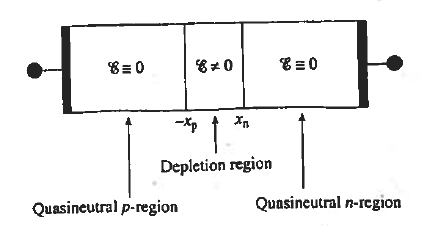
 ………..(1)Equation (1) is identical to the ideal diode equation if VA is set equal to kT/q. In addition to essentially yielding the ideal diode equation, the foregoing analysis very nicely explains how a solid state diode manages to rectify a signal; it, how the diode passes a large current when forward biased and a very small current when reverse biased. Forward biasing reduces the potential hill between the two sides of the junction, permitting _ large numbers of majority carriers to be injected across the depletion region. Reverse biasing increases the potential hill, cutting off majority carrier injection and leaving only a residual current supplied by minority carriers.Once, after completing the qualitative derivation and feeling rather smug about the insight provided, the author was asked. "Yes, but, doesn't the injection of majority carriers under forward bias and the extraction of minority carriers under reverse bias cause a charge build-up inside the device?" The immediate answer is that Steady state conditions were assumed in the analysis and a charge build-up, or a change of any type, does not occur under steady state conditions. The question, however, has deeper implications. The author concentrating solely on the carrier activity in the immediate vicinity of the depletion region, had failed to provide an overall view of carrier activity inside the device. It is the overall view that explains how injected and extracted carriers are resupplied. Q 14) Derive ideal diode equation also explain the boundary conditions? A 14)QUANTITATIVE DERIVATIONBasic Assumptions (1) The diode is being operated under steady state conditions. (2) A non-degenerately doped step junction models the doping profile. (3) The diode is one-dimensional. (4) Low-level injection prevails in the quasineutral regions. (5) There are no processes other than drift, diffusion, and thermal recombination—generation taking place inside the diode. Specifically, GL = O. The preceding assumptions seem reasonable since they were all explicitly or implicitly invoked in establishing the pn junction electrostatics. Let us next consider the general relationships available for computing the current. They are
|
|
|
|
|
 |thermal R-G =0,
  |thermal R-G =0We get dJN(x)/dx = 0 and dJP(x)/dx = 0. JN and JP are therefore determined to be constants independent of position inside the depletion region. The constancy of the carrier currents throughout the depletion region, thus we obtain
  ……… (12)JN(-xp) and JP(xn) can be evaluated at the edges of the depletion region. Thus we have
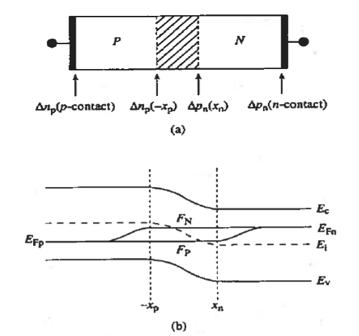
 ………(13)The critical assumption that thermal recombination-generation is negligible in the depletion region can be viewed as a defining property of the ideal diode. Boundary Conditions The minority carrier diffusion equations require boundary conditions in order to solve. In particular, the excess minority carrier concentrations must be known at the edges of the semiconductor – at the contacts as well as the depletion region boundary.Two boundary conditions are required At the Ohmic Contacts:The ideal diode is usually taken to be a "wide-base" diode. In a wide-base diode any perturbation in the carrier concentrations created at the edges of the depletion region will decay to zero before reaching the contacts. The contacts may effectively be viewed as being positioned at x =
 so. Thus, in the mathematical derivation
|
 ………(14)At the Depletion Region Edges: To establish the boundary conditions at the edges of the depletion region, we make use of the quasi-Fermi level formalism. We know
 ………(15)One does not know the variation of the quasi-Fermi levels as a function of position prior to solving for the carrier concentrations inside the diode. However, as envisioned in Figure 18(b), it is reasonable to assume the FN and F, levels will vary monotonically from EFp far on the p- side of the junction to EFn far on the n-side of the junction. Note from Figure 18(b), that the monotonic variation in the levels in turn makes FN— FP
  EFn - EFp = qVA at all points inside the diode. If the equal sign in the preceding expression for FN— FP is assumed to hold throughout the depletion region, one concludes
  ………(16)Eq. (16) has been referred to as the "law of the junction." Evaluating Eq. (6.12) at the depletion region edges very rapidly leads to the desired boundary conditions. Specifically, evaluating Eq. (16) at the p-edge of the depletion region gives
Similarly at n edge
|
subject to the boundary conditions
The general solution is
where
|
|
 as
as  . the only way that the Eq. (24) boundary condition can be satisfied is for A2 to be identically zero. With A2= 0, application of the Eq. (25) boundary condition yields A2= 0). We therefore conclude
and
………(29)
and
………(31) All that remains is to evaluate Ens. (29) and (31) at the depletion region edges. sum the results, and multiply by A. We find
………(32)
………(33)
……… (34)
……… (35)
|
|
|
|
|
|
|
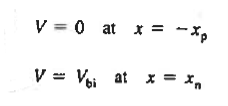 ……….(9)Separating variables and integrating from the depletion region edge to an arbitrary point x, one obtains for the p-side of the depletion region
For n side
|
 …………(14) Solution for xp and xnThe electrostatic solution is not complete until the values of xp and xn are determined. Specifically, xp and xn are the only unknowns in Equations (7) and (14). Using (7) in (14) we can found xn.
And after solving further the value of xp comes to be Thus we get
|
 0 and VA
  0?A 16)Step Junction with VA
  For the practical purpose the solution for the electrostatic variables must be extended to VA
  .Consider the diode in Figure 12 with a voltage VA
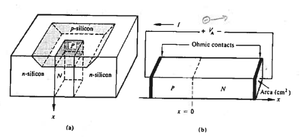
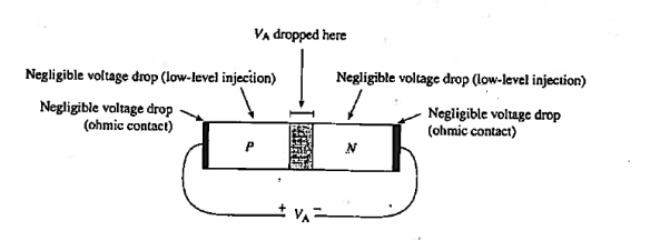
  applied to the diode terminals. This voltage must be dropped somewhere inside the diode. However, in a well-made device a negligible portion of the applied voltage appears across the contacts to the device. More-over, under low-level injection conditions (reasonable current levels) the resistive voltage drop across the quasineutral p- and n-regions extending from the contacts to the edges of the depletion region will also be negligible. The applied voltage must therefore be dropped across the depletion region. When VA> 0. this externally imposed voltage drop lowers the potential on the n-side of the junction relative to the p-side of die junction. Conversely, when VA < 0, the potential on the n-side increases relative to the p-side.
|
 electrostatic relationships can be extrapolated from the VA = 0 relationships by simply replacing all explicit appearances of Vbi by Vbi - VA. Making the indicated substitution yields the VA
  solution for the electrostatic variables given in Equations.For -xp
  x
x 0
0
For
Thus depletion width become
|
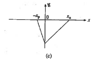
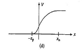
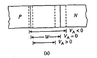
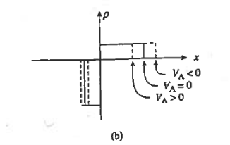
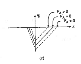
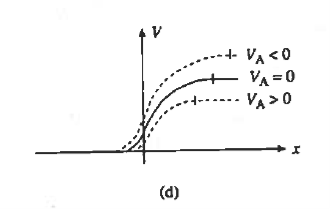
 Vbi in Equations (20), (23) and (24). The formulation fails because a large current begins to flow, and quasineutral region voltage drops cannot he neglected, when VA approaches Vbi.Let us see how the electrostatic variables change as a function of the applied bias. Examining the (20) and (23) relationships for xp and xn, we conclude these widths decrease under forward biasing (VA > 0) and increase under reverse biasing ( VA < 0).The changes in xp and xn likewise translate into changes in the electric field. As deduced from Equations (18) and (21), a smaller xp and xn under forward biases cause the ξ -field to decrease everywhere inside the depletion region while-the larger xp and xn associated with reverse biases give rise to a larger ξ -field. This conclusion is also reasonable from a physical standpoint. A decreased depletion width when VA > 0 means less charge around the junction and a correspondingly smaller ξ-field. On the other hand VA<0, creates a larger space charge region and a bigger electric field,The potential given by Equations (19) and (22) decreases at all points when VA > 0 and increases at all points when VA < 0. The potential hill shrinks in both size and x-extent under forward biasing, whereas reverse biasing gives rise to a wider and higher potential hill. This is summarized graphically in figure 13.
|
|
|
|
|
