|
|
|
|
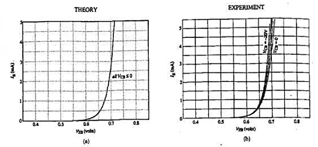
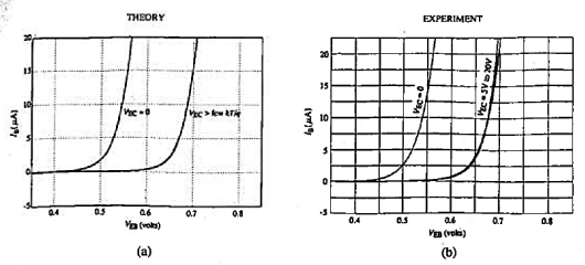
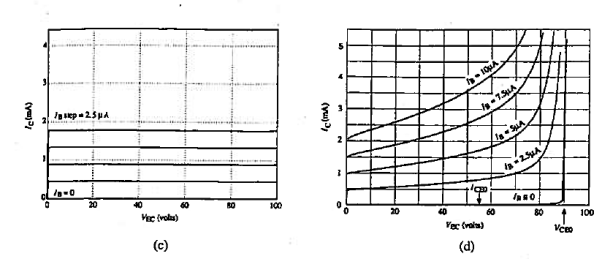
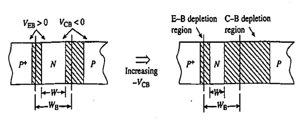
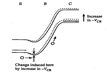
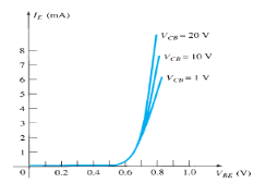
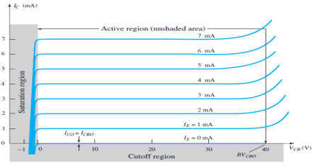
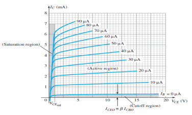
 ………. (2)Where the reverse bias applied to the C—B junction increases, the C—B depletion width increases and W decreases. IE at a given VEB is expected to increase with increasing -VCB. This is the result we obtain in the experimental characteristics shown in Figure 15(b). Base width modulation is also responsible for the quasilinear increase in the common emitter output current recorded in figure 16(d). Under active mode biasing common-emitter output characteristics reduces to
  ……….(3)
where
 is given by
  ……….(4)Since W decreases with increasing reverse bias across the C-B junction,
  systematically increases with increasing VEC. Thus, with base width modulation taken into account, the IC at a given IB under active mode biasing is likewise expected to increase with increasing VEC. It should be noted that base width modulation does not explain the sharp upturn in IC as the output voltage approaches VCE0. Under active mode common base output characteristics is given by
  ………. (5)where
  is given by
  ………. (6)In a well-made transistor the W-dependent terms in the denominator of the as expression are small compared to unity. As a result, even large changes in W give rise to an almost unnoticeable change in
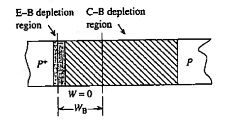
  . The ICB0 is W-independent and is moreover negligible in most instances.Let us see the effect of transistor doping and the biasing mode on the sensitivity of base width modulation.In a standard transistor NE >> NB >NC Thus almost all of the E-B depletion region lies in the base and most of the C-B depletion legion lies in the collector. Under active mode biasing the E-B junction experiences only a small forward bias and plays a negligible role in modulating the quasineutral width of the base. The C-B junction is when subjected to a large reverse bias. The effect of base width modulation is minimized, however, because most of the C-B depletion region lies in the collector.The opposite is true if the same transistor is operated in the inverted mode. In the inverted mode a reverse bias is applied across the E-B junction, the associated depletion width extends almost exclusively into the base, and the standard transistor is inherently quite sensitive to base width modulation. Q 3) What do you meant by punch-through?A 3) Punch-through might be viewed as base width modulation carried to the extreme. Specifically, it refers to the physical situation where base width modulation has resulted in W
  0. Punch through is the condition when the base is said to be punched through when the E-B and C-B depletion regions touch inside the base as shown in Figure 18(a)
|
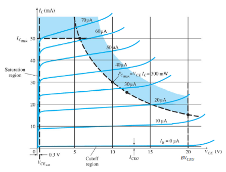
 , where M is the multiplication factor Assuming avalanche breakdown takes place before punch-through, the maximum magnitude of the voltage that can be applied to the output of the BJT under common base operation, VCB0, is clearly just the breakdown voltage of the C-B junction. Common Emitter The common emitter case is far more interesting. The output voltage applied to a transistor connected in the common emitter configuration is VEC = VEB - VCBUnder active mode biasing, the E-B junction is forward biased and VEB is typically quite small.Thus for output voltages exceeding a few volts, we haveVEC = - VCBFrom this it is to be expected thatVCE0
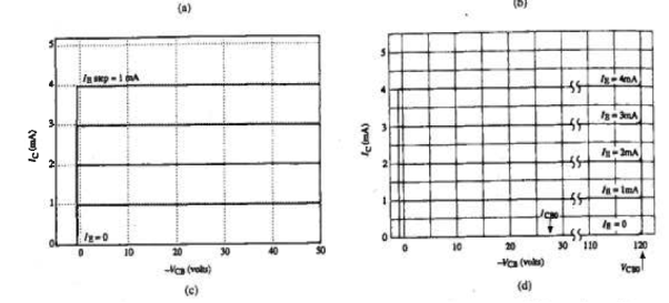
  VCB0However, examining the experimental characteristics one finds a VCE0 considerably smaller than VCB0; VCE0
  90V, whereas VCB0
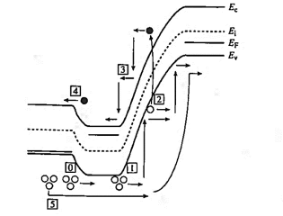
 120VThis unexpected result can be explained qualitatively with the help of Figure 19. The initial injection of holes into the base, labelled as
  in the figure leads to the holes labelled as [1] entering the base-side of the C-B depletion region. Although the C-B junction is biased with voltage less than breakdown voltage, a few of these holes gain a sufficient amount of energy to impact ionize semiconductor atoms and create extra holes and electrons [2]. The added holes drift along with the injected holes into the collector; the added electrons are swept into the base labelled as [3] .
|
 ) >
) >  dc +1 additional holes flow into the collector. Effectively, the carrier multiplication in the C-B depletion region is internally amplified under common emitter operation. Moreover, the process we have just described is regenerative; i.e., it feeds back on itself. With added injection there is added carrier multiplication in the C-B depletion region and an even larger enhancement of the collector current. This all leads to an instability point where Ic
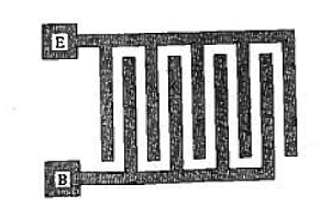
  at a VEC far below the avalanche breakdown voltage of the C-B junction.Q 5) Explain geometrical effects for BJT?A 5) GEOMETRICAL EFFECTS We have assumed the bipolar transistor to be "one-dimensional." with all currents primarily restricted to flowing in one direction. It is obvious the current flow patterns must be decidedly more complex. This leads to several deviations from the ideal of a geometrical nature. Included under "geometrical effects" are internal voltage drops directly associated with the three-dimensional character of the current. Emitter Area
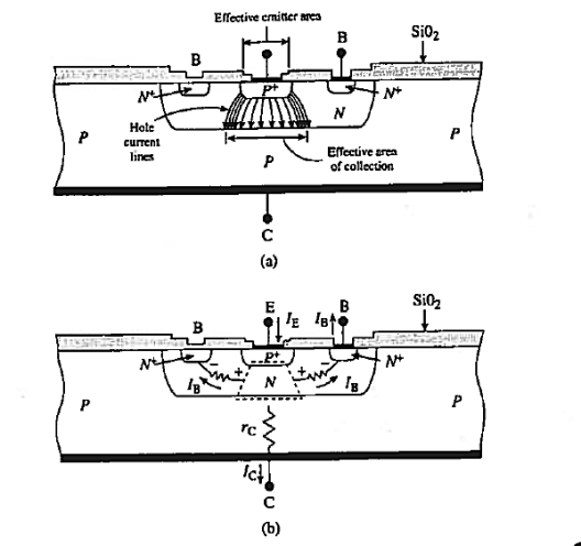
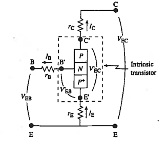
  Collector AreaIn the ideal model, carriers injected from the emitter into the base are assumed to travel in a straight line to the collector. The current flow path in an actual transistor can have a considerable lateral component. This is illustrated in Figure 20(a) using the cross section of a discrete planar transistor. The spread in current can be approximately taken into account by employing different effective areas for the emitter and collector.Series Resistances The base current flowing between the base contact and the "heart" of the transistor must pass through a resistive bulk region [the dashed line region in Figure 20(b). There is also a small resistance associated with the base contact itself. This means the voltage drop across the E—B junction is somewhat less than the VEB terminal voltage. Although typically quite small in magnitude, the voltage difference is often significant because the E—B junction is forward biased under active mode operation and the emitter current is an exponential function of the junction voltage. To account for the voltage difference, one introduces a base series resistance, rB, equal to the sum of the bulk and contact resistances. If rB is the only series resistance of importance, then we used V’EB instead of VEBV’EB = VEB - IBrB
|
|
|
|
or
|
When we substituted into equations (3) and (4)
|
This allows us to write
|
and
|
 F and IF0 constants independent of bias and
and
With g11 = g22 = 0 we obtain the desired result. We also conclude gm
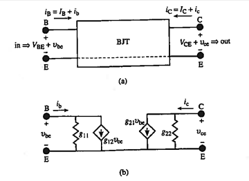
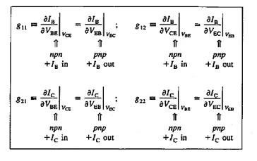
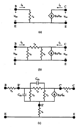
gm and rπ can be calculated using operating point. The four-element low-frequency model of Figure 24(b) is used when base-width modulation cannot be ignored or a more precise analysis is to be performed. Circuit parameters can be related to the two-port model parameters in a straightforward fashion.
|
|
|
|
|
|
|
|
|
|
|
|
|
|
|
Sr.no | Parameter | CB | CE | CC |
1 | Common terminal betnI/p & o/p | Base | Emitter | collector |
2 | Input Current | IE | IB | IB |
3 | Output Current | IC | IC | IE |
4 | Current Gain |
|
| ɤ= |
5 | Input Vtg. | VEB | VBE | VBC |
6 | Output Vtg. | VCB | VCE | VCC |
 =
=  =
=  for pnp BJT ………… (1)0
  and the current gain in a BJT is maximized by making
  as close as possible to unity. Base Transport Factor The fraction of the minority carriers injected into the base that successfully diffuse across the quasineutral width of the base and enter the collector is known as the base transport factor
  . In a pnp BJT the number of carriers injected into the base from the emitter is proportional to the residual number of carriers entering the collector is proportional to
  . The fraction making it across the base is therefore
 =
=  for pnp BJT ………… (2)0
  The smaller the loss of injected carriers via recombination in the quasineutral base, the smaller the degradation of BJT performance and the larger
  . When
  is close to unity maximum amplification occurs.Q 12) What do you meant by term Common Base d.c. Current Gain and Common Emitter d.c. Current?A 12) Common Base d.c. Current GainIn the common base configuration, the active mode ( -VCB > 0) portion of the output characteristics is accurately modeled by the relationship
  ………… (3)where
  is the common base d.c. current gain and
  is the collector current that flows when
  . Making use of Eqs. (1) and (2), we got
 ………… (4)and
 ………… (5)Comparing Eqs. (3) and (5). we conclude
  ………… (6)and
 ………… (7)Eq (6) is significant in that it relates the external gain en of the BJT to the internal performance parameters. Also 0
  Common Emitter d.c. CurrentWhen connected in the common emitter configuration, the active mode portion of the output characteristics is modeled by the relationship
  ………… (8)where
  is the common base d.c. current gain and
  is the collector current that flows when
  . A second relationship between
  and
and  can be established by substituting
  =
=  +
+  into Eq. (3).
 ………… (9)On solving we have
  ………… (10)On comparing Eqs (8) and (10) we get
 ………… (11)and
 ………… (12)also
 ………… (13)
 is negligible compared to Ic. the specified operating point. Equation (11) is significant because it indicates that
  can always be calculated from the value of
  Since
Since  is typically close to unity and
  >>
>>  and
and  is to be expected.