Unit - 5
Unit - 5
Semiconductor memories and Programmable logic devices
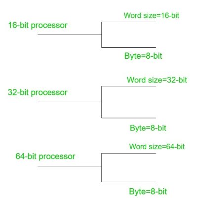
Q1) Define memory request ad word size.
A1)
Memory Request:
Memory request contains the address along with the control signals. For Example, When inserting data into the stack, each block consumes memory (RAM) and the number of memory cells can be determined by the capacity of a memory chip.
Word Size:
It is the maximum number of bits that a CPU can process at a time and it depends upon the processor. Word size is a fixed size piece of data handled as a unit by the instruction set or the hardware of a processor.
Q2) Explain ROM and its types.
A2)
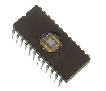
- ROM stands for Read Only Memory.
- It can only read but cannot write on it.
- This memory is non-volatile.
- The information is stored permanently during manufacturing.
- It stores instructions that are required to start a computer and is referred to as bootstrap.
- They are not only used in the computer but also in other electronic devices like washing machine, microwave oven etc.
Advantages:
- Non-volatile in nature
- Cheaper than RAMs
- Easy to test
- More reliable
Types:
- Programmable Read-Only Memory (PROM)
- Electrically Programmable Read-Only Memory (EPROM)
- Electrically Erasable Programmable Read-Only Memory (EEPROM; also called Flash ROM)
- Electrically Alterable Read-Only Memory (EAROM)
They are often referred to as programmable ROM. It was designed for specific data which contains the start-up code.
Q3) What is RAM? Explain.
A3)
RAM (Random Access Memory) is the internal memory of the CPU which is used for storing data, program, and result. It is a read-write memory which stores data only if the machine is working and as the machine is switched off, data gets erased.
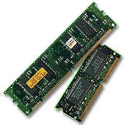
Access time is independent of the address hence each storage location inside the memory is easy to reach and takes the same amount of time. Here, Data can be accessed randomly and is very expensive.
RAM is volatile in nature therefore data stored in it is lost when we switch off the computer or in case of power failure.
Hence, a Uninterruptible Power System (UPS) is used as a backup with computers. RAM is small in size and in the amount of data it can hold.
Q4) What is CAM? Explain.
A4)
Content-addressable memory (CAM) is silicon chip architecture that is purpose-built for extremely fast but very specific type of memory lookups. Lookups using a CAM is conceptually similar to associative array logic in data structures but the output are highly simplified. When key is passed to a CAM sub-system it returns the associated value to that key. As a result, a “key -> value” pair is created that can be referenced further as an object. The most important feature is that a lookup of an entry in a CAM can be performed in a single clock cycle in the silicon. Compare this with a RAM module that requires multiple clock cycles to make a single memory fetch.
Q5) Write a short note on CAM and CCD.
A5)
CCD
A charge coupled device (CCD) is an integrated circuit etched onto a silicon surface forming light sensitive elements called pixels. Photons incident on this surface generate charge that can be read by electronics and turned into a digital copy of the light patterns falling on the device. CCDs come in a wide variety of sizes and types and are used in many applications from cell phone cameras to high-end scientific applications.
CAM
Content-addressable memory (CAM) is silicon chip architecture that is purpose-built for extremely fast but very specific type of memory lookups. Lookups using a CAM is conceptually similar to associative array logic in data structures but the output are highly simplified. When key is passed to a CAM sub-system it returns the associated value to that key. As a result, a “key -> value” pair is created that can be referenced further as an object. The most important feature is that a lookup of an entry in a CAM can be performed in a single clock cycle in the silicon. Compare this with a RAM module that requires multiple clock cycles to make a single memory fetch.
Q6) Give example and explain PLA in detail.
A6)
- Programmable Logic Array (PLA) is a fixed architecture logic device with programmable AND gates followed by programmable OR gates.
- It is basically a type of programmable logic device used to build reconfigurable digital circuit.
- PLDs have undefined function at the time of manufacturing but they are programmed before made into use.
- PLA is a combination of memory and logic.
- PLA is similar to a ROM in concept; however it does not provide full decoding of variables and does not generate all min terms as in the ROM.
- It does not require any type of programming like in C and C++.
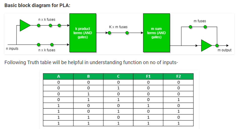
F1 = AB’C’ + AB’C + ABC’ + ABC
On simplifying we get : F1 = AB’ + AC
F2 = A’BC + AB’C + ABC
On simplifying we get: F2 = BC + AC
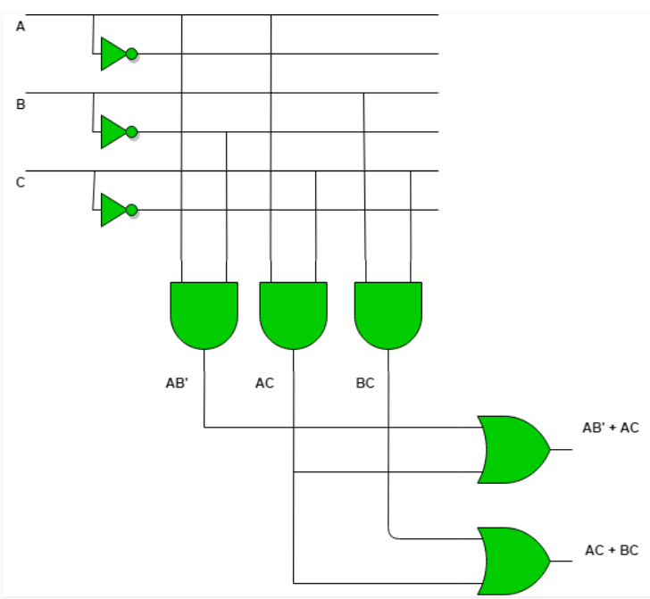
Q7) Implement the following Boolean expression with the help of programmable array logic (PAL)
X =AB + AC’
Y= AB’ + BC’
A7)
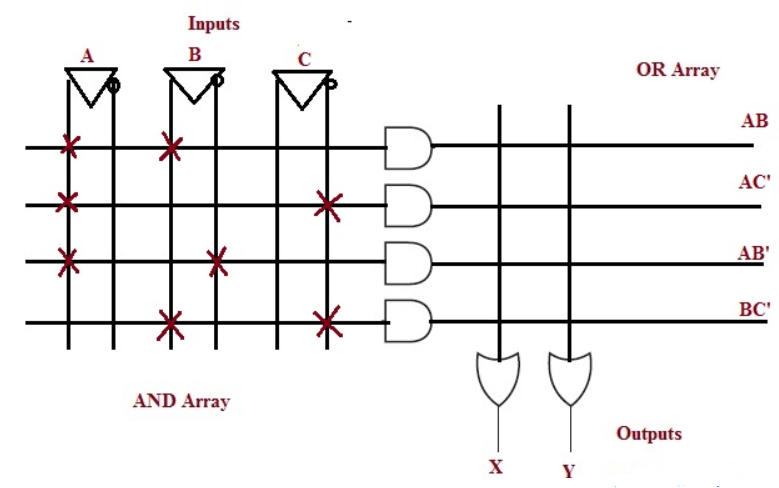
Q8) Comparison between PLA and PAL
A8)
Programmable Array Logic (PAL) | Programmable Logic Array (PLA) |
The full form of PAL is programmable array logic | The full form of the PLA is a programmable logic array |
The construction of PAL can be done using the programmable collection of AND & OR gates | The construction of PLA can be done using the programmable collection of AND & fixed collection of OR gates. |
The availability of PAL is less prolific | The availability of PLA is more |
The flexibility of PAL programming is more | The flexibility of PLA is less |
The cost of a PAL is expensive | The cost of PLA is middle range |
The number of functions implemented in PAL is large | The number of functions implemented in PLA is limited |
The speed of PAL is slow | The speed of PLA is high |
Q9) Write short note on CPLD.
A9)
A complex programmable logic device comprises of a group of programmable FBs (functional blocks). The inputs and outputs of these functional blocks are connected together by a GIM (global interconnection matrix). This interconnection matrix is reconfigurable, so that we can modify the contacts between the functional blocks. There will be some input and output blocks that let us to unite CPLD to external world. The architecture of CPLD is shown below.
Generally, the programmable FB looks like the array of logic gates, where an array of AND gates can be programmed and OR gates are stable. But, each manufacturer has their way of thinking to design the functional block. A listed o/p can be found by operating the feedback signals attained from the OR gate outputs.
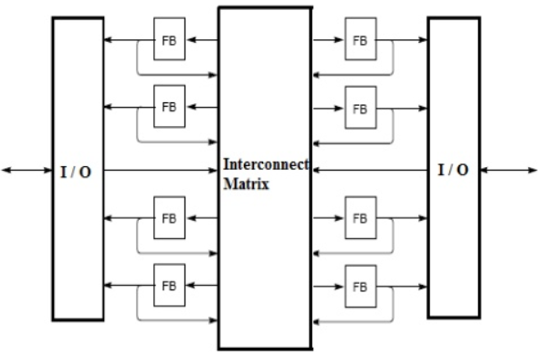
Fig.: CPLD architecture
In CPLD programming, the design is first coded in Verilog or VHDL language once the code is (simulated and synthesized. During synthesis, the CPLD model (target device) is handpicked and a technology-based mapping net list is produced. This list can be close-fitting to the genuine CPLD architecture using a place and route process, typically achieved by the place-and-route software of CPLD Company’s proprietary. Then the operator will do some confirmation processes. If everything is good, he will utilize the CPLD, else he will rearrange it.
Q10) Compare CPLD and FPGA
A10)
| CDLD | FPGA |
1 | Instant-on. CPLDs start working as soon as they are powered up | Since FPGA has to load configuration data from external ROM and setup the fabric before it can start functioning, there is a time delay between power ON and FPGA starts working. The time delay can be as large as several tens of milliseconds. |
2 | Non-volatile. CPLDs remain programmed, and retain their circuit after powering down. FPGAs go blank as soon as powered-off. | FPGAs uses SRAM based configuration storage. The contents of the memory is lost as soon as power is disconnected. |
3 | Deterministic Timing Analysis. Since CPLDs are comparatively simpler to FPGAs, and the number of interconnects are less, the timing analysis can be done much more easily. | Size and complexity of FPGA logic can be humongous compared to CPLDs. This opens up the possibility less deterministic signal routing and thus causing complicated timing scenarios. Thankfully implementation tools provided by FPGA vendors have mechanisms to assist achieving deterministic timing. But additional steps by the user is usually necessary to achieve this. |
4 | Lower idle power consumption. Newer CPLDs such as CoolRunner-II use around 50 uA in idle conditions. | Relatively higher idle power consumption. |
5 | Might be cheaper for implementing simpler circuits | FPGAs are much more capable compared to CPLDs but can be more expensive as well. |
6 | More "secure" due to design storage within built in non-volatile memory. | FPGAs that use external memory can expose the IP externally. Many FPGA vendors offer mechanisms such as encryption to combat this. Design specific protection mechanisms also can be implemented. |
7 | Very small amount of logic resources. | Massive amount logic and storage elements, with which incredibly complex circuits can be designed. FPGAs have thousands of times more resources! This point alone makes FPGAs more popular than CPLDs. |
8 | No on-die hard IPs available to offload processing from the logic fabric. | Variety of on-die dedicated hardware such as Block RAM, DSP blocks, PLL, DCMs, Memory Controllers, Multi-Gigabit Transceivers etc give immense flexibility. This is not even thinkable with CPLDs. |
9 | Power down and reprogramming is always required in order to modify design functionality. | FPGAs can change their circuit even while running! (Since it is just a matter of updating LUTs with different content) This is called Partial Reconfiguration, and is very useful when FPGAs need to keep running a design and at the same time update the it with different design as per requirement. This feature is widely used in Accelerated Computing. |