UNIT 2
Operational amplifier and its applications
Q1. Give a brief introduction on operational amplifiers?
A1.

The block diagram of op-amp consists of :
Non-inverting input
Inverting input
It has a dual input.
It is a differential amplifier which provides balanced output.
It provides voltage gain.
Establishes input resistance of op-amp.
It also has a dual input.
It is a differential amplifier which provides unbalanced output.
The output of the input stage becomes input for the intermediate stage.
Due to direct coupling, the dc voltage is well above 0V.
The output of the intermediate stage becomes input for the level shifting stage.
It is an emitter follower with constant current source.
It is used to shift dc level at the output to 0V wrto ground.
This is the final stage.
It’s a push pull amplifier.
It raises swing in output voltage as well as increases current supply capability of op-amp.
Q2. What do you understand by Op-amp input modes and parameters?
A2. Open Loop Gain, (Avo)
Infinite – The main function of an operational amplifier is to amplify the input signal and the more open loop gain it has the better. Open-loop gain is the gain of the op-amp without positive or negative feedback and for such an amplifier the gain will be infinite but typical real values range from about 20,000 to 200,000.
Input impedance, (ZIN)
Infinite – Input impedance is the ratio of input voltage to input current and is assumed to be infinite to prevent any current flowing from the source supply into the amplifiers input circuitry ( IIN = 0 ). Real op-amps have input leakage currents from a few pico-amps to a few milli-amps.
Output impedance, (ZOUT)
Zero – The output impedance of the ideal operational amplifier is assumed to be zero acting as a perfect internal voltage source with no internal resistance so that it can supply as much current as necessary to the load. This internal resistance is effectively in series with the load thereby reducing the output voltage available to the load. Real op-amps have output impedances in the 100-20kΩ range.
Bandwidth, (BW)
Infinite – An ideal operational amplifier has an infinite frequency response and can amplify any frequency signal from DC to the highest AC frequencies so it is therefore assumed to have an infinite bandwidth. With real op-amps, the bandwidth is limited by the Gain-Bandwidth product (GB), which is equal to the frequency where the amplifiers gain becomes unity.
Offset Voltage, (VIO)
Zero – The amplifiers output will be zero when the voltage difference between the inverting and the non-inverting inputs is zero, the same or when both inputs are grounded. Real op-amps have some amount of output offset voltage.
Q3. Explain the function of Op-amp in open loop configuration?
A3. “Open Loop Gain” which is defined as the amplifiers output amplification without any external feedback signals connected to it and for a typical operational amplifier is about 100dB at DC (zero Hz). This output gain decreases linearly with frequency down to “Unity Gain” or 1, at about 1MHz and this is shown in the following open loop gain response curve.
Open-loop Frequency Response Curve
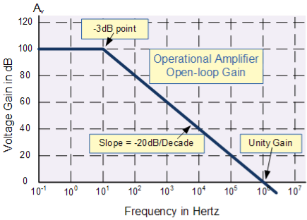
From this frequency response curve we can see that the product of the gain against frequency is constant at any point along the curve. Also that the unity gain (0dB) frequency also determines the gain of the amplifier at any point along the curve. This constant is generally known as the Gain Bandwidth Product or GBP. Therefore:
GBP = Gain x Bandwidth = A x BW
For example, from the graph above the gain of the amplifier at 100kHz is given as 20dB or 10, then the gain bandwidth product is calculated as:
GBP = A x BW = 10 x 100,000Hz = 1,000,000.
Similarly, the operational amplifiers gain at 1kHz = 60dB or 1000, therefore the GBP is given as:
GBP = A x BW = 1,000 x 1,000Hz = 1,000,000.
The Voltage Gain (AV) of the operational amplifier can be found using the following formula:
Av = Vout/ Vin
and in Decibels or (dB) is given as:
20 log (A) or 20 log (Vout/ Vin ) in dB
An Op- Amp Bandwidth
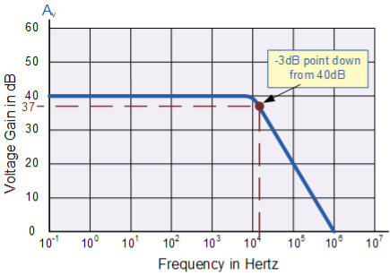
The operational amplifiers bandwidth is the frequency range over which the voltage gain of the amplifier is above 70.7% or -3dB (where 0dB is the maximum) of its maximum output value.
Example
Using the formula 20 log (A), we can calculate the bandwidth of the amplifier as:
37 = 20 log (A) therefore, A = anti-log (37 ÷ 20) = 70.8
GBP ÷ A = Bandwidth, therefore, 1,000,000 ÷ 70.8 = 14,124Hz, or 14kHz
Then the bandwidth of the amplifier at a gain of 40dB is given as 14kHz as previously predicted from the graph.
Q4. Explain the process of Op-amp with negative feedback?
A4.
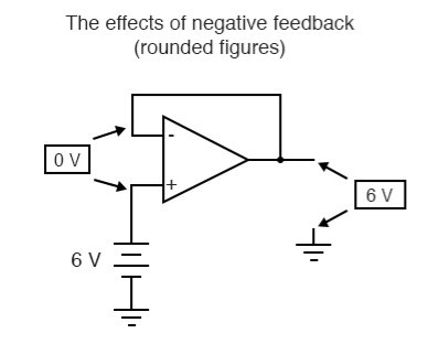
If we connect the output of an op-amp to its inverting input and apply a voltage signal to the noninverting input, we find that the output voltage of the op-amp closely follows that input voltage (I’ve neglected to draw in the power supply, +V/-V wires, and ground symbol for simplicity):

As Vin increases, Vout will increase in accordance with the differential gain. However, as Vout increases, that output voltage is fed back to the inverting input, thereby acting to decrease the voltage differential between inputs, which acts to bring the output down. What will happen for any given voltage input is that the op-amp will output a voltage very nearly equal to Vin, but just low enough so that there’s enough voltage difference left between Vin and the (-) input to be amplified to generate the output voltage.
The circuit will quickly reach a point of stability (known as equilibrium in physics), where the output voltage is just the right amount to maintain the right amount of differential. Taking the op-amp’s output voltage and coupling it to the inverting input is a technique known as negative feedback, and it is the key to having a self-stabilizing system (this is true not only of op-amps, but of any dynamic system in general). This stability gives the op-amp the capacity to work in its linear (active) mode, as opposed to merely being saturated fully “on” or “off” as it was when used as a comparator, with no feedback at all.
Because the op-amp’s gain is so high, the voltage on the inverting input can be maintained almost equal to Vin. Let’s say that our op-amp has a differential voltage gain of 200,000. If Vin equals 6 volts, the output voltage will be 5.999970000149999 volts. This creates just enough differential voltage (6 volts - 5.999970000149999 volts = 29.99985 µV) to cause 5.999970000149999 volts to be manifested at the output terminal, and the system holds there in balance. As you can see, 29.99985 µV is not a lot of differential, so for practical calculations, we can assume that the differential voltage between the two input wires is held by negative feedback exactly at 0 volts.

Q5. Explain in brief the Study of practical op-amp IC 741?
A5. The IC 741 is a small chip. It comprises eight pins. 2, 3 and 6 numbered pins are most significant.
Pin 2 is inverting terminal.
Pin 3 is non-inverting terminal.
Pin 6 is output terminal.
IC 741 mainly performs mathematical operations like addition, subtraction, division, multiplication, integration, differentiation etc. IC 741 has three stages such as differential input, gain, and push-pull output.
Pin 1 and 5 are “offset null” or “balance” terminals.
The op amp is nothing but a differential amplifier. When we apply the same
voltage at the inverting terminal (Pin 2) and the non-inverting terminal (Pin 3) there should not be any voltage at the output terminal (Pin 6). This condition is an ideal.
Practically there is always a small voltage (offset voltage) appears at pin 6 even the voltage applied at pin 2 and 3 are exactly equal. Offset voltage appears at output because we cannot make the parameters of transistors and value of biasing resistances of differential amplifier perfectly same.

Q6. What do you understand by Inverting and non-inverting amplifier?
A6. Inverting amplifier
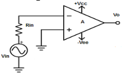
V1 = 0V and V2 = Vin
Vout = A( - Vin )
where, A is the voltage gain of op-amp.
Non-Inverting Amplifier
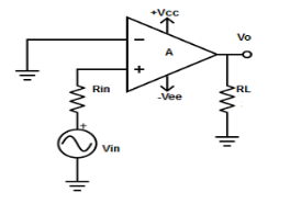
V1 = Vin and V2 = 0V
Vout =AVin
where, A is the voltage gain of op-amp.
Q7. Write a short note on Summer Amplifier?
A7.
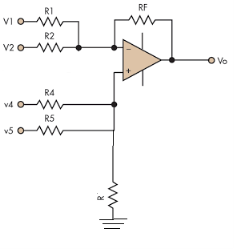


Hence,


Similarly,

So, the resultant output voltage by all the 4 input voltages is given by,
Vo = V01 + V02 + V04 +V05
Vo = -V1 – V2 +V4 + V5
The output voltage Vo is equivalent to the sum all input voltages applied at both the terminals.
Q8. In a summing amplifier, if R = 1kΩ, Va = +3V, Vb = +8V, Vc = +9V, Vd = +5V and supply voltage is ±15V. Find the output voltage Vo.
A8. Vo = Sum of all input voltages applied at both the terminals
Vo = Va + Vb + Vc +Vd
Vo = -3 -8 +9 +5
Vo = +3V
Q9. Find the output voltage for the given circuit diagram if Rf = 5kΩ.
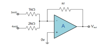
A9.
We know,
Gain (Av) = =
= 
Hence,
Av1 = 
Av2 = 
Now, Output voltage Vo = Sum of the two amplified input signals
Vo = Av1 x V1 + Av2 x V2
Vo =(-5 x 3) + ( -2.5x 4) mV
Vo = -25mV
As the above output voltage is negative hence it is an inverting amplifier.
Q10. Explain the work of Difference Amplifier?
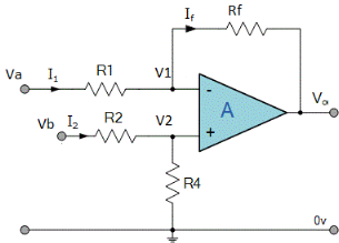
Fig. : Difference amplifier


Summing point, V1 = V2 and
V2 = Vb
If Vb = 0 then 
And Va = 0 then 
Vo = -V01 + V02
Vo =  +
+ 
If R1 = R2 and Rf = R4 then

And if R1 = R2 = Rf = R4 =R then
Vo = Vb – Va
Hence, is known as a Unity Gain Differential Amplifier.
Q11. Explain the working process of Integrator?
A11.
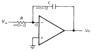

Ignoring I3 we have, I3 ≈ 0
So, I1 ≈ I2.


However, V = 0 because gain A is very large

Integrating both sides we get


 + Q
+ Q
Where Q is the integration constant and is proportional to Vo at t = 0 sec .
Therefore, voltage Vo is directly proportional to Vin and inversely proportional to constant RC.
Frequency response of basic integrator circuit is given by,
 ( for 0 db gain)
Q12. Give a short note on Differentiator?
A12.
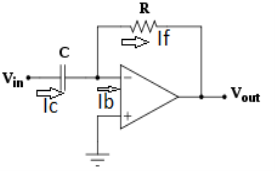
Fig.: Differentiator

Since Ib = 0 then,
Ic ≈ If

Since Gain A is very large hence, V1 = 0

Or 
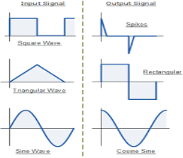
Fig.: Input and output waveform of differentiator (Ref. 1)
 ( for 0 db gain)