UNIT 4
Digital Electronics Fundamentals
Q1. Write the Difference between analog and digital signals?
Analog | Digital |
An analog signal is a continuous signal that represents physical measurements. | Digital signals are time separated signals which are generated using digital modulation. |
It is denoted by sine waves | It is denoted by square waves |
It uses a continuous range of values that help you to represent information. | Digital signal uses discrete 0 and 1 to represent information. |
Temperature sensors, FM radio signals, Photocells, Light sensor, Resistive touch screen are examples of Analog signals. | Computers, CDs, DVDs are some examples of Digital signal. |
The analog signal bandwidth is low | The digital signal bandwidth is high. |
Analog signals are deteriorated by noise throughout transmission as well as write/read cycle. | Relatively a noise-immune system without deterioration during the transmission process and write/read cycle. |
Analog hardware never offers flexible implementation. | Digital hardware offers flexibility in implementation. |
It is suited for audio and video transmission. | It is suited for Computing and digital electronics. |
Processing can be done in real-time and consumes lesser bandwidth compared to a digital signal. | It never gives a guarantee that digital signal processing can be performed in real time. |
Analog instruments usually have s scale which is cramped at lower end and gives considerable observational errors. | Digital instruments never cause any kind of observational errors. |
Analog signal doesn't offer any fixed range. | Digital signal has a finite number, i.e., 0 and 1. |
Q2. Give a short note on Boolean algebra.
A2. Boolean Algebra is used to analyze and simplify the digital (logic) circuits. It uses only the binary numbers i.e. 0 and 1. It is also called as Binary Algebra or logical Algebra. Boolean algebra was invented by George Boole in 1854.
Rule in Boolean Algebra
Following are the important rules used in Boolean algebra.


Q3. Write a description on Basic and Universal Gates?
A3. The basic gates are namely AND gate, OR gate & NOT gate.
AND gate
It is a digital circuit that consists of two or more inputs and a single output which is the logical AND of all those inputs. It is represented with the symbol ‘.’.
The following is the truth table of 2-input AND gate.
A | B | Y = A.B |
0 | 0 | 0 |
0 | 1 | 0 |
1 | 0 | 0 |
1 | 1 | 1 |
Here A, B are the inputs and Y is the output of two input AND gate.
If both inputs are ‘1’, then only the output, Y is ‘1’. For remaining combinations of inputs, the output, Y is ‘0’.
The figure below shows the symbol of an AND gate, which is having two inputs A, B and one output, Y.

Fig. : AND gate (ref. 1)
Timing Diagram:

OR gate
It is a digital circuit which has two or more inputs and a single output which is the logical OR of all those inputs. It is represented with the symbol ‘+’.
The truth table of 2-input OR gate is:
A | B | Y = A + B |
0 | 0 | 0 |
0 | 1 | 1 |
1 | 0 | 1 |
1 | 1 | 1 |
Here A, B are the inputs and Y is the output of two input OR gate.
When both inputs are ‘0’, then only the output, Y is ‘0’. For remaining combinations of inputs, the output, Y is ‘1’.
The figure below shows the symbol of an OR gate, which is having two inputs A, B and one output, Y.

Fig. : OR gate (ref. 1)
Timing Diagram:

NOT gate
It is a digital circuit that has one input and one output. Here the output is the logical inversion of input. Hence, it is also called as an inverter.
The truth table of NOT gate is:
A | Y = A’ |
0 | 1 |
1 | 0 |
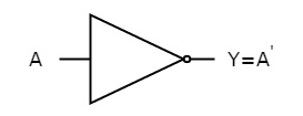
Here A and Y are the corresponding input and output of NOT gate. When A is ‘0’, then, Y is ‘1’. Similarly, when, A is ‘1’, then, Y is ‘0’.
The figure below shows the symbol of NOT gate, which has one input, A and one output, Y.

Fig. : NOT gate (ref. 1)
Timing Diagram:

Universal gates
NAND gate
It is a digital circuit which has two or more inputs and single output and it is the inversion of logical AND gate.
The truth table of 2-input NAND gate is:
A | B | Y = (A.B)’ |
0 | 0 | 1 |
0 | 1 | 1 |
1 | 0 | 1 |
1 | 1 | 0 |
Here A, B are the inputs and Y is the output of two input NAND gate. When both inputs are ‘1’, then the output, Y is ‘0’. If at least one of the input is zero, then the output, Y is ‘1’. This is just the inverse of AND operation.
The image shows the symbol of NAND gate:
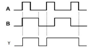
Fig.: NAND gate (ref. 1)
NAND gate works same as AND gate followed by an inverter.
Timing Diagram:
NOR gate
It is a digital circuit that has two or more inputs and a single output which is the inversion of logical OR of all inputs.
The truth table of 2-input NOR gate is:
A | B | Y = (A+B)’ |
0 | 0 | 1 |
0 | 1 | 0 |
1 | 0 | 0 |
1 | 1 | 0 |
Here A and B are the two inputs and Y is the output. If both inputs are ‘0’, then the output is ‘1’. If any one of the input is ‘1’, then the output is ‘0’. This is exactly opposite to two input OR gate operation.
The symbol of NOR gate is:

Fig.: NOR gate (ref. 1)
NOR gate works exactly same as that of OR gate followed by an inverter.
Timing Diagram:

Special Gates
Ex-OR gate
It stands for Exclusive-OR gate. Its function varies when the inputs have even number of ones.
The truth table of 2-input Ex-OR gate is:
A | B | Y = A⊕B |
0 | 0 | 0 |
0 | 1 | 1 |
1 | 0 | 1 |
1 | 1 | 0 |
Here A, B are the inputs and Y is the output of two input Ex-OR gate. The output (Y) is zero instead of one when both the inputs are one.
Therefore, the output of Ex-OR gate is ‘1’, when only one of the two inputs is ‘1’. And it is zero, when both inputs are same.
The symbol of Ex-OR gate is as follows:

Fig.: XOR gate (ref. 1)
It is similar to that of OR gate with an exception for few combination(s) of inputs. Hence, the output is also known as an odd function.
Timing Diagram:

Ex-NOR gate
It stands for Exclusive-NOR gate. Its function is same as that of NOR gate except when the inputs having even number of ones.
The truth table of 2-input Ex-NOR gate is:
A | B | Y = A⊙B |
0 | 0 | 1 |
0 | 1 | 0 |
1 | 0 | 0 |
1 | 1 | 1 |
Here A, B are the inputs and Y is the output. It is same as Ex-NOR gate with the only modification in the fourth row. The output is 1 instead of 0, when both the inputs are one.
Hence the output of Ex-NOR gate is ‘1’, when both inputs are same and 0, when both the inputs are different.
The symbol of Ex-NOR gate is:
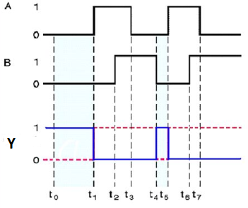
Fig.: XNOR gate (ref. 1)
It is similar to NOR gate except for few combination(s) of inputs. Here the output is ‘1’, when even number of 1 is present at the inputs. Hence is also called as an even function.
Timing Diagram:

Q4. Short note on Logic IC’s.
A4.
Q5. What do you understand by Half and full adder?
A5.
It is a combinational circuit which has two inputs and two outputs.
It is designed to add two single bit binary number A and B.
It has two outputs carry and sum.
Block diagram
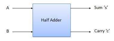
Fig. : Half adder (ref. 2)
Truth Table
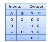
Circuit Diagram
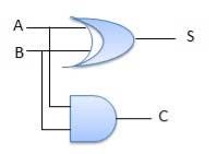
Fig.: Half adder (ref. 2)
Full Adder
It is developed to overcome the drawback of Half Adder circuit.
It can add two one-bit numbers A and B and a carry C.
It is a three input and two output combinational circuit.
Block diagram
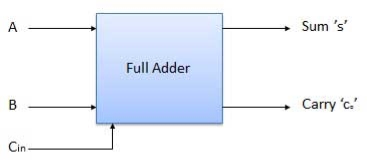
Fig. : Full adder (ref. 2)
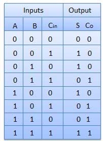
Circuit Diagram
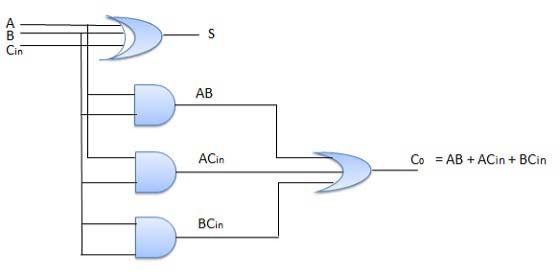
Fig. : Full adder (ref. 2)
Q6. Explain the work of Multiplexers?
A6.
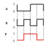
Fig.: Block diagram of multiplexer (ref. 2)
Multiplexers come in multiple variations
Block Diagram of 2:1 MUX
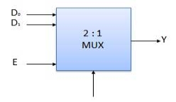
Truth Table of 2:1 MUX

Where x is don’t care.
Q7.Explain the function of De-multiplexers?
A7.
Various Demultiplexers are used as:
Block diagram
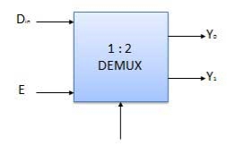
Truth Table

Where x is don’t care.
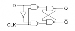
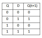
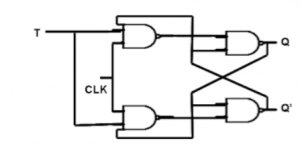
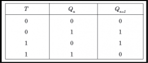
Q8. What do you understand by Flip-flops?
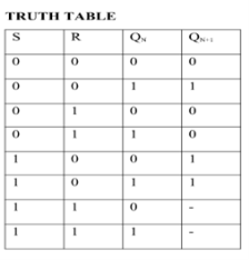
A8. SR Flip Flop

JK Flip Flop

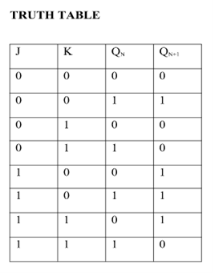
Race Around Condition In JK Flip-flop –
D Flip Flop
T Flip Flop
Q9. Give a short note on Shift registers.
A9.
The registers which shift the bits towards right are called “Shift right registers”.
Shift registers are of 4 types and they are:
Serial-In Serial-Out Shift Register (SISO) –

Fig. SISO
Serial-In Parallel-Out shift Register (SIPO) –

Fig. SIPO
Parallel-In Serial-Out Shift Register (PISO) –
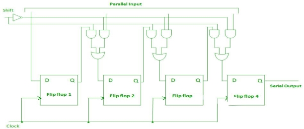
Fig. PISO
Parallel-In Parallel-Out Shift Register (PIPO) –
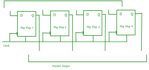
Fig. PIPO
Q10. Write in brief about the function of Counters?
A10.
Counter Classification
Counters are broadly classified into two categories:
1. Asynchronous Counter

Fig. Asynchronous counter
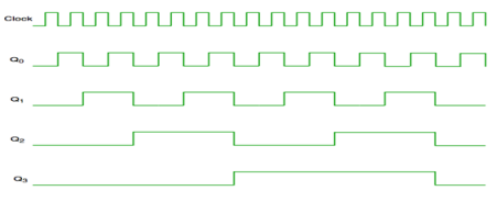
Fig. Timing diagram of Asynchronous counter
2. Synchronous Counter
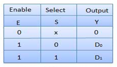
Fig. synchronous counter
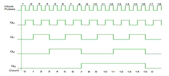
Fig. Timing diagram of synchronous counter
Q11. What do you understand by microprocessor/microcontroller and explain its application?
A11. Microprocessor: Introduction
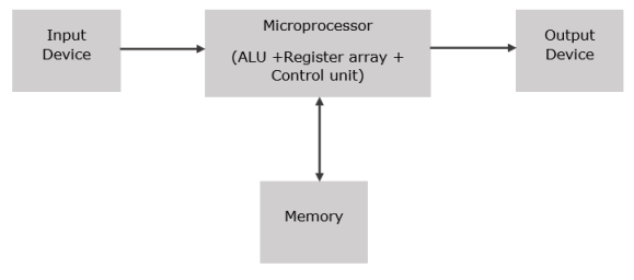
Fig.: Basic block diagram of microprocessor
Microcontroller: Introduction

