Unit - 1
MOS Field-Effect Transistor
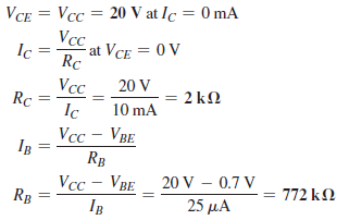
Q1) Determine the values of VCC RC and RB of a fixed bias configuration for a given load line and defined Q point.

A1)
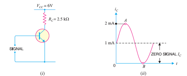
Q2) A npn silicon transistor has VCC = 6 V and the collector load RC = 2.5 kΩ. Find: (i) The maximum collector current that can be allowed during the application of signal for faithful amplification. (ii) The minimum zero signal collector current required.
A2)
A2)
Collector supply voltage, VCC = 6 V
Collector load, RC = 2.5 Kω
(i) We know that for faithful amplification, VCE should not be less than 1V for silicon transistor.
∴ Max. voltage allowed across RC = 6 − 1 = 5 V
∴ Max. allowed collector current = 5 V/RC = 5 V/2.5 kΩ = 2 mA
Thus, the maximum collector current allowed during any part of the signal is 2 mA. If the collector current is allowed to rise above this value, VCE will fall below 1 V. Consequently, value of β will fall, resulting in unfaithful amplification.
(ii) During the negative peak of the signal, collector current can at the most be allowed to become zero. As the negative and positive half cycles of the signal are equal, therefore, the change in collector current due to these will also be equal but in opposite direction.
∴ Minimum zero signal collector current required = 2 mA/2 = 1 mA
During the positive peak of the signal [point A in Fig. 1(ii)], iC = 1 + 1 = 2mA
And during the negative peak (point B), iC = 1 − 1 = 0 mA
Q3) A transistor employs a 4 kΩ load and VCC = 13V. What is the maximum input signal if β = 100? Given Vknee = 1V and a change of 1V in VBE causes a change of 5mA in collector current.
A3) Collector supply voltage, VCC = 13 V
Knee voltage, Vknee = 1 V
Collector load, RC = 4 kΩ
∴ Max. allowed voltage across RC = 13 − 1 = 12 V
∴ Max. allowed collector current, iC =12 V /RC = 12 V/ 4 KΩ = 3 mA
Maximum base current, iB = iC / β = 3 mA / 100 = 30 μA
Now collector-current / Base voltage (signal voltage) = 5 mA/V
∴Base voltage (signal voltage) = Collector current / (5 mA/V) = 3 mA / (5 mA/V) = 600 mV
Q4) Fig. (i) shows biasing with base resistor method. (i) Determine the collector current IC and collector-emitter voltage VCE. Neglect small base-emitter voltage. Given that β = 50. (ii) If RB in this circuit is changed to 50 kΩ, find the new operating point.
A4)

In the circuit shown in Fig. (i), biasing is provided by a battery VBB (= 2V) in the base circuit which is separate from the battery VCC (= 9V) used in the output circuit.
The same circuit is shown in a simplified way in Fig. 2 (ii). Here, we need show only the supply voltages, + 2V and +9V. It may be noted that negative terminals of the power supplies are grounded to get a complete path of current.
IB RB + VBE = 2
IB = 20 A
A
IC =  IB = 50x20
 A= 1mA
IC RC + VCE = 9
VCE = 9- (1mA x 2000) = 7V
When RB is made equal to 50k
IC =  IB = 50x40
 A= 2mA
VCE = 9- (2mA x 2000) = 5V
So, the operating point is 5V and 2mA
Q5) Fig. 3 (i) shows that a silicon transistor with β = 100 is biased by base resistor method. Draw the d.c. load line and determine the operating point. What is the stability factor?
A5)
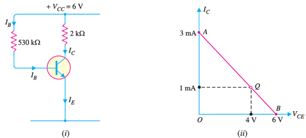
Here, VCC = 6 V, RB = 530 kΩ, RC = 2 kΩ
D.C. load line
Referring to Fig. 3 (i), VCE = VCC − ICRC
When IC = 0,
VCE = VCC = 6 V. This locates the first point B (OB = 6V) of the load line on collector-emitter voltage axis as shown in Fig. 3 (ii).
When VCE = 0,
IC = VCC/RC = 6V/2 kΩ = 3 mA.
This locates the second point A (OA = 3mA) of the load line on the collector current axis. By joining points A and B, d.c. load line AB is constructed as shown in Fig. 3(ii).
Operating point Q
As it is a silicon transistor, therefore, VBE = 0.7V.
IB RB +VBE =VCC
IB = (6-0.7)/530x103 =10 A
A
IC =  IB = 100x10= 1mA
VCE = 6- (1mA x 2000) = 4V
The operating point is 4V, 1mA.
The stability factor is given by  +1 = 100+1 =101
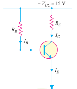
Q6) Design base resistor bias circuit for a CE amplifier such that operating point is VCE = 8V and IC = 2 mA. You are supplied with a fixed 15V d.c. supply and a silicon transistor with β = 100. Take base-emitter voltage VBE = 0.6V. Calculate also the value of load resistance that would be employed.
Fig. shows CE amplifier using base resistor method of biasing.
A6)
VCC = 15v
β = 100
VBE = 0.6V
VCE = 8V, IC = 2 mA.
VCC = VCE + IC RC
15 = 8+ 2mAxRC
RC = 3.5k
IC =  IB
IB
IB = 2/100 =0.02mA
VCC = IB RB + VBE
RB = (15-0.6)/ (0.02x10⁻³) = 720k
Q7) In base bias method, how Q-point is affected by changes in VBE and ICBO.
A7) In addition to being affected by change in β, the Q-point is also affected by changes in VBE and ICBO in the base bias method.
(i) Effect of VBE:
The base-emitter-voltage VBE decreases with the increase in temperature (and vice-versa). The expression for IB in base bias method is given by;
IB = VCC – VBE/RB
It is clear that decrease in VBE increases IB. This will shift the Q-point (IC = βIB and VCE = VCC – IC RC). The effect of change in VBE is negligible if VCC >> VBE (VCC at least 10 times greater than VBE).
(ii) Effect of ICBO:
The reverse leakage current ICBO has the effect of decreasing the net base current and thus increasing the base voltage. It is because the flow of ICBO creates a voltage drop across RB that adds to the base voltage as shown in Fig. 6. Therefore, change in ICBO shifts the Q-point of the base bias circuit.

However, in modern transistors, ICBO is usually less than 100 nA and its effect on the bias is negligible if VBB >> ICBO RB.
Q8) For figure below is a resistor transistor circuit. The device has the characteristics as shown below. Find VCC, RC and RB?
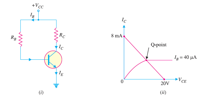
A8) The DC Line voltage VCC = 20V
Maximum IC = VCC/RC
RC = 20/8x10-3=2.5k
IB = VCC – VBE/RB
RB = 20-0.7/40x10-6 = 482.5k
Q9) Determine IDQ, VGSQ, VD, VS, VDS, and VDG?

A9) VG = VDDR2/R1+R2 = (16x270K)/(2.1M+270K) = 1.823V
VGS = 1.823- ID RS = 1.823 – 1.5x10³ ID
ID = IDSS (1-VGS/VP)2 = 8x10⁻³ (2.12-1092ID+140625ID2)
1125 ID2-9.736ID+0.01696=0
ID= 2.417mA
Discard other value as its not feasible.
VDS= VDD -ID (RD + RS) = 16- 2.417x10⁻³(2.4K+1.5K) = 6.5737V
VGS = 1.823- ID RS = 1.823 – (1.5x103x2.417x10-3) = -1.8025V
V= = ID RS = 2.417x10-3 x 1.5x103 = 3.6255V
VD = VDD – ID RD = 16- 2.417x10⁻³(2.4K) = 10.2V
VDG = VD – VG = 10.2 – 1.823 =8.377V
Q10) Calculate the value of feedback resistor Rs required to self-bias JFET with IDSS= 40mA, VP= -10 and VGSQ= -5V?
A10) IDQ =IDSS [1-(VGSQ/VP)]2
= 40x10-3 [1- {(-5)/ (-10)}]2 = 10mA
For self-bias VGSQ = - IDQ RS
RS = -VGSQ/IDQ = -(-5)/10mA = 500Ohm
Q11) For the circuit shown below the FET has VP= 4V, IDSS = 4mA. Calculate IDSQ, VGSQ and VDSQ?

A11)
The simplified circuit will be

VG = R2 VDD/ (R1 + R2) = (200x10-3x(-60))/(1.3x106+200x103) = -8V
VG – VGS +ID RS = 0
VGS = -8 + ID RS
Finding ID
ID = IDSS (1-VGS/VP)2 = 2.25mA or 4mA
As the given circuit is of p-channel FET so VDS should be negative. For ID =2.25mA the value of VDS is negative.
VDS= VDD -ID (RD + RS) = -60-(-2.25m (4000+18000)) = -10.5V
VGS = -8 +ID R= = 1V
Q12) Compare the biasing of MOSFET and FET?
A12)

Q13) What are factors affecting bias stabilization?
A13) Stabilization of the operating point has to be achieved due to the following reasons.
Let us understand these concepts in detail.
Temperature Dependence of IC
As the expression for collector current IC is
IC=βIB+ICEO
=βIB+(β+1) ICBO
The collector leakage current ICBO is greatly influenced by temperature variations. To come out of this, the biasing conditions are set so that zero signal collector current IC = 1 mA. Therefore, the operating point needs to be stabilized i.e., it is necessary to keep IC constant.
Individual Variations
As the value of β and the value of VBE are not same for every transistor, whenever a transistor is replaced, the operating point tends to change. Hence it is necessary to stabilize the operating point.
Thermal Runaway
As the expression for collector current IC is
IC=βIB+ICEO
=βIB+(β+1) ICBO
The flow of collector current and also the collector leakage current causes heat dissipation. If the operating point is not stabilized, there occurs a cumulative effect which increases this heat dissipation. The self-destruction of such an unstabilized transistor is known as Thermal run away. In order to avoid thermal runaway and the destruction of transistor, it is necessary to stabilize the operating point, i.e., to keep IC constant.
Q14) What is Stability Factor?
A14) It is understood that IC should be kept constant in spite of variations of ICBO or ICO. The extent to which a biasing circuit is successful in maintaining this is measured by Stability factor. It denoted by S.
By definition, the rate of change of collector current IC with respect to the collector leakage current ICO at constant β and IB is called Stability factor.
S=dIC/dICOS at constant IB and β
Hence, we can understand that any change in collector leakage current changes the collector current to a great extent. The stability factor should be as low as possible so that the collector current doesn’t get affected. S=1 is the ideal value.
The general expression of stability factor for a CE configuration can be obtained as under.
IC=βIB+(β+1) ICO
Differentiating above expression with respect to IC, we get
1=βdIB/dIC+(β+1) dICO/dIC
Or
1=βdIB/dIC+(β+1)/S
Since dICO/dIC=1/S
Or
S=β+1/[1−β(dIB/dIC)]
Hence the stability factor S depends on β, IB and IC
Q15) What is faithful amplification?
A15)
The operating point should not get disturbed as it should remain stable to achieve faithful amplification. Hence the quiescent point or Q-point is the value where the Faithful Amplification is achieved.
The process of increasing the signal strength is called as Amplification. This amplification when done without any loss in the components of the signal, is called as Faithful amplification.
Faithful amplification is the process of obtaining complete portions of input signal by increasing the signal strength. This is done when AC signal is applied at its input.
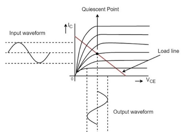
Fig: Amplification with AC input Signal
In the above graph, the input signal applied is completely amplified and reproduced without any losses.
This can be understood as Faithful Amplification.
The operating point is so chosen such that it lies in the active region and it helps in the reproduction of complete signal without any loss.
If the operating point is considered near saturation point, then the amplification will be as under.
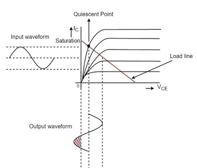
Fig. Operating point near saturation point
If the operation point is considered near cut off point, then the amplification will be as under.
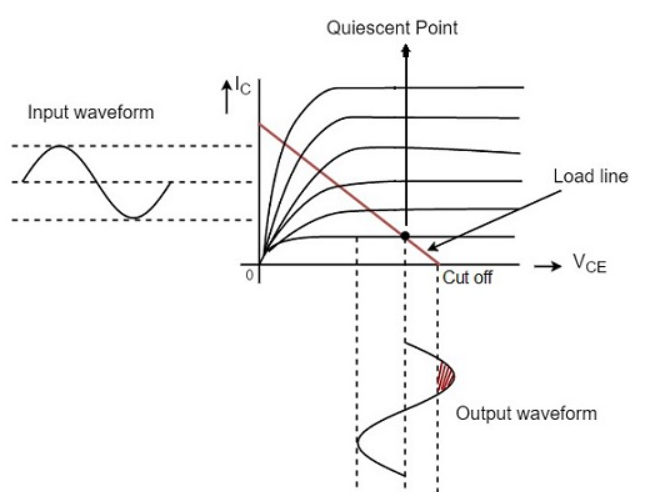
Fig. Operating point near cut-off point
Hence the placement of operating point is an important factor to achieve faithful amplification. But for the transistor to function properly as an amplifier, its input circuit (i.e., the base-emitter junction) remains forward biased and its output circuit (i.e., collector-base junction) remains reverse biased.
Q16) Compare BJT, FET and MOSFET?
A16)
TERMS | BJT | FET | MOSFET |
Device type | Current controlled | Voltage controlled | Voltage Controlled |
Current flow | Bipolar | Unipolar | Unipolar |
Terminals | Not interchangeable | Interchangeable | Interchangeable |
Operational modes | No modes | Depletion mode only | Both Enhancement and Depletion modes |
Input impedance | Low | High | Very high |
Output resistance | Moderate | Moderate | Low |
Operational speed | Low | Moderate | High |
Noise | High | Low | Low |
Thermal stability | Low | Better | High |