Unit - 1
Functional blocks of a computer
Q1) What is CPU?
A1) Central Processing Unit (CPU)
A Central Processing Unit is also called a processor, central processor, or microprocessor. It carries out all the important functions of a computer. It receives instructions from both the hardware and active software and produces output accordingly. It stores all important programs like operating systems and application software. CPU also helps Input and output devices to communicate with each other. Owing to these features of the CPU, it is often referred to as the brain of the computer.
CPU is installed or inserted into a CPU socket located on the motherboard. Furthermore, it is provided with a heat sink to absorb and dissipate heat to keep the CPU cool and functioning smoothly.
Generally, a CPU has three components:
● ALU (Arithmetic Logic Unit)
● Control Unit
● Memory or Storage Unit
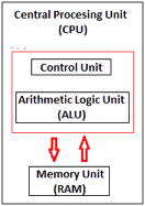
Fig 1 - CPU
Control Unit: It is the circuitry in the control unit, which makes use of electrical signals to instruct the computer system for executing already stored instructions. It takes instructions from memory and then decodes and executes these instructions. So, it controls and coordinates the functioning of all parts of the computer. The Control Unit's main task is to maintain and regulate the flow of information across the processor. It does not take part in processing and storing data.
ALU: It is the arithmetic logic unit, which performs arithmetic and logical functions. Arithmetic functions include addition, subtraction, multiplication division, and comparisons. Logical functions mainly include selecting, comparing, and merging the data. A CPU may contain more than one ALU. Furthermore, ALUs can be used for maintaining timers that help run the computer.
Memory or Storage Unit/ Registers: It is called Random access memory (RAM). It temporarily stores data, programs, and intermediate and final results of processing. So, it acts as a temporary storage area that holds the data temporarily, which is used to run the computer.
What is CPU Clock Speed?
The clock speed of a CPU or a processor refers to the number of instructions it can process in a second. It is measured in gigahertz. For example, a CPU with a clock speed of 4. 0 GHz means it can process 4 billion instructions in a second.
Q2) Write the types of CPU?
A2) Types of CPU
CPUs are mostly manufactured by Intel and AMD, each of which manufactures its types of CPUs. In modern times, there are lots of CPU types in the market. Some of the basic types of CPUs are described below:
Single Core CPU: Single Core is the oldest type of computer CPU, which was used in the 1970s. It has only one core to process different operations. It can start only one operation at a time; the CPU switches back and forth between different sets of data streams when more than one program runs. So, it is not suitable for multitasking as the performance will be reduced if more than one application runs. The performance of these CPUs is mainly dependent on the clock speed. It is still used in various devices, such as smartphones.
Dual-Core CPU: As the name suggests, Dual Core CPU contains two cores in a single Integrated Circuit (IC). Although each core has its controller and cache, they are linked together to work as a single unit and thus can perform faster than the single-core processors and can handle multitasking more efficiently than Single Core processors.
Quad-Core CPU: This type of CPU comes with two dual-core processors in one integrated circuit (IC) or chip. So, a quad-core processor is a chip that contains four independent units called cores. These cores read and execute instructions of the CPU. The cores can run multiple instructions simultaneously, thereby increases the overall speed for programs that are compatible with parallel processing.
Quad-Core CPU uses a technology that allows four independent processing units (cores) to run in parallel on a single chip. Thus, by integrating multiple cores in a single CPU, higher performance can be generated without boosting the clock speed. However, the performance increases only when the computer's software supports multiprocessing. The software which supports multiprocessing divides the processing load between multiple processors instead of using one processor at a time.
Q3) Write the history of CPU?
A3) History of CPU
Some of the important events in the development of CPU since its invention till date are as follows:
● In 1823, Baron Jons Jackob Berzelius discovered silicon that is the main component of the CPU to date.
● In 1903, Nikola Tesla got gates or switches patented, which are electrical logic circuits.
● In December 1947, John Bardeen, William Shockley, and Walter Brattain invented the first transistor at the Bell Laboratories and got it patented in 1948.
● In 1958, the first working integrated circuit was developed by Robert Noyce and Jack Kilby.
● In 1960, IBM established the first mass-production facility for transistors in New York.
● In 1968, Robert Noyce and Gordon Moore founded Intel Corporation.
● AMD (Advanced Micro Devices) was founded in May 1969.
● In 1971, Intel introduced the first microprocessor, the Intel 4004, with the help of Ted Hoff.
● In 1972, Intel introduced the 8008 processor; in 1976, Intel 8086 was introduced, and in June 1979, Intel 8088 was released.
● In 1979, a 16/32-bit processor, the Motorola 68000, was released. Later, it was used as a processor for the Apple Macintosh and Amiga computers.
● In 1987, Sun introduced the SPARC processor.
● In March 1991, AMD introduced the AM386 microprocessor family.
● In March 1993, Intel released the Pentium processor. In 1995, Cyrix introduced the Cx5x86 processor to give competition to Intel Pentium processors.
● In January 1999, Intel introduced the Celeron 366 MHz and 400 MHz processors.
● In April 2005, AMD introduced its first dual-core processor.
● In 2006, Intel introduced the Core 2 Duo processor.
● In 2007, Intel introduced different types of Core 2 Quad processors.
● In April 2008, Intel introduced the first series of Intel Atom processors, the Z5xx series. They were single-core processors with a 200 MHz GPU.
● In September 2009, Intel released the first Core i5 desktop processor with four cores.
● In January 2010, Intel released many processors such as Core 2 Quad processor Q9500, first Core i3 and i5 mobile processors, first Core i3 and i5 desktop processors. In the same year in July, it released the first Core i7 desktop processor with six cores.
● In June 2017, Intel introduced the first Core i9 desktop processor.
● In April 2018, Intel released the first Core i9 mobile processor.
Q4) Define computer memory?
A4) Computer Memory
The computer memory holds the data and instructions needed to process raw data and produce output. The computer memory is divided into a large number of small parts known as cells. Each cell has a unique address which varies from 0 to memory size minus one.
Computer memory is of two types: Volatile (RAM) and Non-volatile (ROM). The secondary memory (hard disk) is referred to as storage, not memory.
But, if we categorize memory on behalf of space or location, it is of four types:
● Register memory
● Cache memory
● Primary memory
● Secondary memory
Register Memory
Register memory is the smallest and fastest memory in a computer. It is not a part of the main memory and is located in the CPU in the form of registers, which are the smallest data holding elements. A register temporarily holds frequently used data, instructions, and memory addresses that are to be used by the CPU. They hold instructions that are currently processed by the CPU. All data is required to pass through registers before it can be processed. So, they are used by the CPU to process the data entered by the users.
Registers hold a small amount of data around 32 bits to 64 bits. The speed of a CPU depends on the number and size (no. of bits) of registers that are built into the CPU. Registers can be of different types based on their uses. Some of the widely used Registers include Accumulator or AC, Data Register or DR, the Address Register or AR, Program Counter (PC), I/O Address Register, and more.
Types and Functions of Computer Registers:
● Data Register: It is a 16-bit register, which is used to store operands (variables) to be operated by the processor. It temporarily stores data, which is being transmitted to or received from a peripheral device.
● Program Counter (PC): It holds the address of the memory location of the next instruction, which is to be fetched after the current instruction is completed. So, it is used to maintain the path of execution of the different programs and thus executes the programs one by one, when the previous instruction gets completed.
● Instructor Register: It is a 16-bit register. It stores the instruction which is fetched from the main memory. So, it is used to hold instruction codes, which are to be executed. The Control Unit takes instruction from the Instructor Register, then decodes and executes it.
● Accumulator Register: It is a 16-bit register, which is used to store the results produced by the system. For example, the results generated by the CPU after the processing are stored in the AC register.
● Address Register: It is a 12-bit register that stores the address of a memory location where instructions or data is stored in the memory.
● I/O Address Register: Its job is to specify the address of a particular I/O device.
● I/O Buffer Register: Its job is to exchange the data between an I/O module and the CPU.
Cache Memory
Cache memory is a high-speed memory, which is small in size but faster than the main memory (RAM). The CPU can access it more quickly than the primary memory. So, it is used to synchronize with a high-speed CPU and to improve its performance.
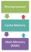
Fig 2 – Memory
Cache memory can only be accessed by the CPU. It can be a reserved part of the main memory or a storage device outside the CPU. It holds the data and programs which are frequently used by the CPU. So, it makes sure that the data is instantly available for the CPU whenever the CPU needs this data. In other words, if the CPU finds the required data or instructions in the cache memory, it doesn't need to access the primary memory (RAM). Thus, by acting as a buffer between RAM and CPU, it speeds up the system performance.
Types of Cache Memory:
L1: It is the first level of cache memory, which is called Level 1 cache or L1 cache. In this type of cache memory, a small amount of memory is present inside the CPU itself. If a CPU has four cores (quad-core CPU), then each core will have its level 1 cache. As this memory is present in the CPU, it can work at the same speed as the CPU. The size of this memory ranges from 2KB to 64 KB. The L1 cache further has two types of caches: The instruction cache, which stores instructions required by the CPU, and the data cache that stores the data required by the CPU.
L2: This cache is known as Level 2 cache or L2 cache. This level 2 cache may be inside the CPU or outside the CPU. All the cores of a CPU can have their separate level 2 cache, or they can share one L2 cache among themselves. In case it is outside the CPU, it is connected with the CPU with a very high-speed bus. The memory size of this cache is in the range of 256 KB to 512 KB. In terms of speed, they are slower than the L1 cache.
L3: It is known as Level 3 cache or L3 cache. This cache is not present in all the processors; some high-end processors may have this type of cache. This cache is used to enhance the performance of Level 1 and Level 2 cache. It is located outside the CPU and is shared by all the cores of a CPU. Its memory size ranges from 1 MB to 8 MB. Although it is slower than L1 and L2 cache, it is faster than Random Access Memory (RAM).
How does cache memory work with CPU?
When the CPU needs the data, first of all, it looks inside the L1 cache. If it does not find anything in L1, it looks inside the L2 cache. If again, it does not find the data in the L2 cache, it looks into the L3 cache. If data is found in the cache memory, then it is known as a cache hit. On the contrary, if data is not found inside the cache, it is called a cache miss.
If data is not available in any of the cache memories, it looks inside the Random Access Memory (RAM). If RAM also does not have the data, then it will get that data from the Hard Disk Drive.
So, when a computer is started for the first time, or an application is opened for the first time, data is not available in cache memory or RAM. In this case, the CPU gets the data directly from the hard disk drive. Thereafter, when you start your computer or open an application, the CPU can get that data from cache memory or RAM.
Primary Memory
Primary Memory is of two types: RAM and ROM.
RAM (Volatile Memory)
It is a volatile memory. It means it does not store data or instructions permanently. When you switch on the computer the data and instructions from the hard disk are stored in RAM.
CPU utilizes this data to perform the required tasks. As soon as you shut down the computer the RAM loses all the data.
ROM (Non-volatile Memory)
It is a non-volatile memory. It means it does not lose its data or programs that are written on it at the time of manufacture. So, it is a permanent memory that contains all important data and instructions needed to perform important tasks like the boot process.
Secondary Memory
The secondary storage devices which are built into the computer or connected to the computer are known as a secondary memory of the computer. It is also known as external memory or auxiliary storage.
The secondary memory is accessed indirectly via input/output operations. It is non-volatile, so it permanently stores the data even when the computer is turned off or until this data is overwritten or deleted. The CPU can't directly access the secondary memory. First, the secondary memory data is transferred to primary memory then the CPU can access it.
Some of the secondary memory or storage devices are described below:
1) Hard Disk:
It is a rigid magnetic disc that is used to store data. It permanently stores data and is located within a drive unit.

Fig 3 – Hard disk
The hard disk is also known as a hard drive. It is a rigid magnetic disc that stores data permanently, as it is a non-volatile storage device. The hard disk is located within a drive unit on the computer's motherboard and comprises one or more platters packed in an air-sealed casing. The data is written on the platters by moving a magnetic head over the platters as they spin. The data stored on a computer's hard drive generally includes the operating system, installed software, and the user's files and programs, including pictures, music, videos, text documents, etc.
Components of Hard Drive:
The main components of a hard drive include a head actuator, read/write actuator arm, read/write head, platter, and spindle. A circuit board, which is called the disk controller or interface board, is present on the back of a hard drive. It allows the hard drive to communicate with the computer.
2) Solid-state Drive:

Fig 4 – SSD
SSD (Solid State Drive) is also a non-volatile storage medium that is used to hold and access data. Unlike a hard drive, it does not have moving components, so it offers many advantages over SSD, such as faster access time, noiseless operation, less power consumption, and more.
As the cost of SSD has come down, it has become an ideal replacement for a standard hard drive-in desktop and laptop computers. It is also suitable for notebooks, and tablets that don't require lots of storage.
3) Pen drive:

Fig 5 – Pen drive
Pen drive is a compact secondary storage device. It is also known as a USB flash drive, thumb drive, or jump drive. It connects to a computer via a USB port. It is commonly used to store and transfer data between computers. For example, you can write a report using a computer and then copy or transfer it to the pen drive. Later, you can connect this pen drive to a computer to see or edit your report. You can also store your important documents and pictures, music, videos in the pen drive and keep them in a safe place.
Pen drive does not have movable parts; it comprises an integrated circuit memory chip that stores the data. This chip is housed inside a plastic or aluminium casing. The data storage capacity of the pen drive generally ranges from 2 GB to 128 GB. Furthermore, it is a plug and play device as you don't need additional drives, software, or hardware to use it.
4) SD Card:

Fig 6 – SD card
SD Card stands for Secure Digital Card. It is most often used in portable and mobile devices such as smartphones and digital cameras. You can remove it from your device and see the things stored in it using a computer with a card reader.
There are many memory chips inside the SD card that store the data; it does not have moving parts. SD cards are not created equal, so they may differ from each other in terms of speed, physical sizes, and capacity. For example, standard SD cards, mini SD cards, and micro SD cards.
5) Compact Disk (CD):

Fig 7 – CD
Compact Disk is a portable secondary storage device in the shape of a round medium disk. It is made of polycarbonate plastic. The concept of CD was co-developed by Philips and Sony in 1982. The first CD was created on 17 August 1982 at the workshop of Philips in Germany.
In the beginning, it was used for storing and playing sound recordings, later it was used for various purposes such as for storing documents, audio files, videos, and other data like software programs in a CD.
Physical characteristics of a CD/ Structure of CD:
A standard CD is around 5 inches in diameter and 0. 05 inches in thickness. It is made of a clear polycarbonate plastic substrate, a reflective metallic layer, and a clear coating of acrylic plastic. These thin circular layers are attached one on top of another as described below:
● A polycarbonate disc layer at the bottom has the data encoded by creating lands and pits.
● The polycarbonate disc layer is coated with a thin aluminium layer that reflects the laser.
● The reflective aluminium layer is coated with a lacquer layer to prevent oxidation to protect the below layers. It is generally spin coated directly on the top of the reflective layer.
● The label print is applied on the lacquer layer, or artwork is screen printed on the top of the disc on the lacquer layer by offset printing or screen printing.
How Does a CD Work?
The data or information is stored or recorded or encoded in CD digitally using a laser beam that etches tiny indentations or bumps on its surface. The bump is called a pit, which represents the number 0. Space, where the bump is not created, is called land, and it represents the number 1. Thus, the data is encoded into a compact disc by creating pits (0) and lands (1). The CD players use laser technology to read the optically recorded data.
6) DVD:

Fig 8 - DVD
DVD is short for digital versatile disc or digital video disc. It is a type of optical media used for storing optical data. Although it has the same size as a CD, its storage capacity is much more than a CD. So, it is widely used for storing and viewing movies and to distribute software programs as they are too large to fit on a CD. DVD was co-developed by Sony, Panasonic, Philips, and Toshiba in 1995.
Types of DVDs:
DVDs can be divided into three main categories which are as follows:
● DVD-ROM (Read-Only): These types of DVDs come with media already recorded on them, such as movie DVDs. As the name suggests, data on these discs cannot be erased or added, so these discs are known as a read-only or non-writable DVD.
● DVD-R (Writable): It allows you to record or write information to the DVD. However, you can write information only once as it becomes a read-only DVD once it is full.
● DVD-RW (Rewritable or Erasable): This type of discs can be erased, written, or recorded multiple times.
Q5) Explain I/O Systems and Subsystems?
A5) I/O Systems and Subsystems
I/O devices are very important in computer systems. They provide users the means of interacting with the system. So, there is a separate I/O system devoted to handling the I/O devices.
The different Components of the I/O systems are −
I/O Hardware
There are many I/O devices handled by the operating system such as a mouse, keyboard, disk drive, etc. Different device drivers can be connected to the operating system to handle a specific device. The device controller is an interface between the device and the device driver.
A diagram to represent this is −
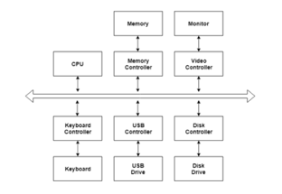
Fig 9 – I/O Hardware
I/O Application Interface
The user applications can access all the I/O devices using the device drivers, which are device-specific codes. The application layer sees a common interface for all the devices.
This is illustrated using the below image −
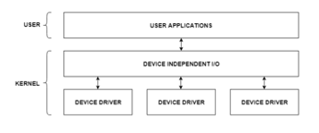
Fig 10 – I/O Application Interface
Most of the devices are either block I/O and character I/O devices. Block devices are accessed one block at a time whereas character devices are accessed one character at a time.
I/O Software
The I/O software contains the user-level libraries and the kernel modules. The libraries provide the interface to the user program to perform input and output. The kernel modules provide the device drivers that interact with the device controllers.
The I/O software should be device-independent so that the programs can be used for any I/O device without specifying it in advance. For example - A program that reads a file should be able to read the file on a hard disk, floppy disk, CD-ROM, etc. without having to change the program each time.
Q6) Define a control unit?
A6) Control unit
During the execution of a program, the control unit fetches one instruction at a time from the main memory and then executes it. In this execution process, it takes the help of ALU, if the instruction execution involves arithmetic or logical operation (like AND, OR, Ex-OR). After the execution of the current instruction, the CPU fetches the next instruction for execution. This process continues until the program is completed and the result is output using the output device. In many computers, the control unit and the ALU are integrated into a single block, known as Central Processing Unit (CPU).
Central Processing Unit (CPU) consists of the following features −
● CPU is considered as the brain of the computer.
● CPU performs all types of data processing operations.
● It stores data, intermediate results, and instructions (program).
● It controls the operation of all parts of the computer.
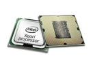
Fig 11 - Processor
The CPU itself has the following three components.
● Memory or Storage Unit
● a control unit
● ALU (Arithmetic Logic Unit)
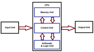
Fig 12 – Control Unit
Memory or Storage Unit
This unit can store instructions, data, and intermediate results. This unit supplies information to other units of the computer when needed. It is also known as an internal storage unit or the main memory or the primary storage or Random-Access Memory (RAM).
Its size affects speed, power, and capability. Primary memory and secondary memory are two types of memories in the computer. Functions of the memory unit are −
● It stores all the data and the instructions required for processing.
● It stores intermediate results of processing.
● It stores the final results of processing before these results are released to an output device.
● All inputs and outputs are transmitted through the main memory.
Control unit
This unit controls the operations of all parts of the computer but does not carry out any actual data processing operations.
Functions of this unit are −
● It is responsible for controlling the transfer of data and instructions among other units of a computer.
● It manages and coordinates all the units of the computer.
● It obtains the instructions from the memory, interprets them, and directs the operation of the computer.
● It communicates with input/output devices for the transfer of data or results from storage.
● It does not process or store data.
ALU (Arithmetic Logic Unit)
This unit consists of two subsections namely,
● Arithmetic section
● Logic Section
Arithmetic section
The function of the arithmetic section is to perform arithmetic operations like addition, subtraction, multiplication, and division. All complex operations are done by making repetitive use of the above operations.
Logic Section
The function of the logic section is to perform logic operations such as comparing, selecting, matching, and merging data.
Q7) Describe Instruction set architecture of a CPU–registers?
A7) Instruction set architecture of a CPU–registers
This means that an ISA describes the design of a computer in terms of the basic operations it must support. The ISA is not concerned with the implementation-specific details of a computer. It is only concerned with the set or collection of basic operations the computer must support. For example, the AMD Athlon and the Core 2 Duo processors have entirely different implementations but they support more or less the same set of basic operations as defined in the x86 Instruction Set.
Let us try to understand the Objectives of an ISA by taking the example of the MIPS ISA. MIPS is one of the most widely used ISAs in education due to its simplicity.
Based on the type of operations they perform MIPS Instructions are classified into 3 types:
● Arithmetic/Logic Instructions:
These Instructions perform various Arithmetic & Logical operations on one or more operands.
● Data Transfer Instructions:
These instructions are responsible for the transfer of instructions from memory to the processor registers and vice versa.
● Branch and Jump Instructions:
These instructions are responsible for breaking the sequential flow of instructions and jumping to instructions at various other locations, this is necessary for the implementation of functions and conditional statements.
2. The ISA defines the maximum length of each type of instruction.
Since the MIPS is a 32-bit ISA, each instruction must be accommodated within 32 bits.
3. The ISA defines the Instruction Format of each type of instruction. The Instruction Format determines how the entire instruction is encoded within 32 bits
There are 3 types of Instruction Formats in the MIPS ISA:
● R-Instruction Format
● I-Instruction Format
● J-Instruction Format
Each of the above Instruction Formats has different instruction encoding schemes, and hence need to be interpreted differently by the processor.
If we look at the Abstraction Hierarchy:
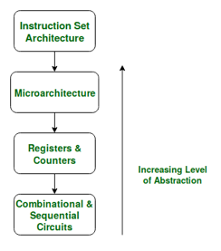
Fig 13 – The Abstraction Hierarchy
We note that the Microarchitectural level lies just below the ISA level and hence is concerned with the implementation of the basic operations to be supported by the computer as defined by the ISA. Therefore, we can say that the AMD Athlon and Core 2 Duo processors are based on the same ISA but have different microarchitectures with different performance and efficiencies.
Now one may ask the need to distinguish between Microarchitecture and ISA?
The answer to this lies in the need to standardize and maintain the compatibility of programs across different hardware implementations based on the same ISA. Making different machines compatible with the same set of basic instructions (The ISA) allows the same program to run smoothly on many different machines thereby making it easier for the programmers to document and maintain code for many different machines simultaneously and efficiently.
This Flexibility is the reason we first define an ISA and then design different microarchitectures complying with this ISA for implementing the machine. The design of an ISA is one of the major tasks in the study of Computer Architecture.
Instruction Set Architecture | Microarchitecture |
The ISA is responsible for defining the set of instructions to be supported by the processor. For example, some of the instructions defined by the ARMv7 ISA are given below. | The Microarchitecture is more concerned with the lower-level implementation of how the instructions are going to be executed and deals with concepts like Instruction Pipelining, Branch Prediction, Out of Order Execution. |
The Branch of Computer Architecture is more inclined towards the Analysis and Design of Instruction Set Architecture. For Example, Intel developed the x86 architecture, ARM developed the ARM architecture, & AMD developed the amd64 architecture. The RISC-V ISA developed by UC Berkeley is an example of an Open-Source ISA. | On the other hand, the Branch of Computer Organization is concerned with the implementation of a particular ISA that deals with various hardware implementation techniques, i. e. is the Microarchitecture level. For Example, ARM licenses other companies like Qualcomm, Apple for using ARM ISA, but each of these companies have their implementations of this ISA thereby making them different in performance and power efficiency. The Krait cores developed by Qualcomm have a different microarchitecture and the Apple A-series processors have a different microarchitecture. |
The x86 was developed by Intel, but we see that almost every year Intel comes up with a new generation of i-series processors. The x86 architecture on which most of the Intel Processors are based essentially remains the same across all these generations but, where they differ is in the underlying Microarchitecture. They differ in their implementation and hence are claimed to have improved Performance. These various Microarchitectures developed by Intel are codenamed as ‘Nehalem’, ‘Sandybridge’, ‘Ivybridge’, and so on.
Therefore, in conclusion, we can say that different machines may be based on the same ISA but have different Microarchitectures.
Q8) What do you mean by Instruction execution cycle?
A8) Instruction execution cycle
A program residing in the memory unit of a computer consists of a sequence of instructions. These instructions are executed by the processor by going through a cycle for each instruction.
In a basic computer, each instruction cycle consists of the following phases:
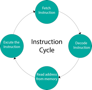
Fig 14 - Input-Output Configuration
In computer architecture, input-output devices act as an interface between the machine and the user.
Instructions and data stored in the memory must come from some input device. The results are displayed to the user through some output device.
The following block diagram shows the input-output configuration for a basic computer.
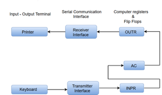
Fig 15 – I/O configuration
● The input-output terminals send and receive information.
● The amount of information transferred will always have eight bits of an alphanumeric code.
● The information generated through the keyboard is shifted into an input register 'INPR'.
● The information for the printer is stored in the output register 'OUTR'.
● Registers INPR and OUTR communicate with a communication interface serially and with the AC in parallel.
● The transmitter interface receives information from the keyboard and transmits it to INPR.
● The receiver interface receives information from OUTR and sends it to the printer serially.
Q9) What is RTL interpretation of instructions?
A9) RTL interpretation of instructions
A digital computer system exhibits an interconnection of digital modules such as registers, decoders, arithmetic elements, and control logic.
These digital modules are interconnected with some common data and control paths to form a completely digital system.
Moreover, digital modules are best defined by the registers and the operations that are performed on the data stored in them.
The operations performed on the data stored in registers are called Micro-operations.
The internal hardware organization of a digital system is best defined by specifying:
● The set of registers and the flow of data between them.
● The sequence of micro-operations performed on the data which are stored in the registers.
● The control paths that initiate the sequence of micro-operation
The Register Transfer Language is the symbolic representation of notations used to specify the sequence of micro-operations.
In a computer system, data transfer takes place between processor registers and memory and between processor registers and input-output systems. These data transfer can be represented by standard notations given below:
● Notations R0, R1, R2. . ., and so on represent processor registers.
● The addresses of memory locations are represented by names such as LOC, PLACE, MEM, etc.
● Input-output registers are represented by names such as DATA IN, DATA OUT, and so on.
● The content of the register or memory location is denoted by placing square brackets around the name of the register or memory location.
Q10) What do you mean by addressing modes?
A10) Addressing Modes
The term addressing modes refers to how the operand of an instruction is specified. The addressing mode specifies a rule for interpreting or modifying the address field of the instruction before the operand is executed.
Addressing modes for 8086 instructions are divided into two categories:
1) Addressing modes for data
2) Addressing modes for branch
The 8086 memory addressing modes provide flexible memory access, allowing you to easily access variables, arrays, records, pointers, and other complex data types. The key to good assembly language programming is the proper use of memory addressing modes.
An assembly language program instruction consists of two parts

Fig 16 - Assembly language program instruction
The memory address of an operand consists of two components:
IMPORTANT TERMS
● The starting address of the memory segment.
● Effective address or Offset: An offset is determined by adding any combination of three address elements: displacement, base, and index.
According to different ways of specifying an operand by 8086 microprocessor, different addressing modes are used by 8086.
Addressing modes used by the 8086 microprocessors are discussed below:
Implied mode: In implied addressing the operand is specified in the instruction itself. In this mode, the data is 8 bits or 16 bits long and data is the part of instruction. Zero address instructions are designed with implied addressing mode.

Example: CLC (used to reset Carry flag to 0)
● Immediate addressing mode (symbol #): In this mode data is present in the address field of instruction. Designed like one address instruction format.
Note: Limitation in the immediate mode is that the range of constants is restricted by the size of the address field.

Example: MOV AL, 35H (move the data 35H into AL register)
Register mode: In register addressing the operand is placed in one of 8 bit or 16-bit general-purpose registers. The data is in the register that is specified by the instruction.
Here one register reference is required to access the data.

Example: MOV AX, CX (move the contents of CX register to AX register)
● Register Indirect mode: In this addressing the operand’s offset is placed in any one of the registers BX, BP, SI, DI as specified in the instruction. The effective address of the data is in the base register or an index register that is specified by the instruction.
Here two register references are required to access the data.

Fig 17 – Register Indirect mode
The 8086 CPUs let you access memory indirectly through a register using the register indirect addressing modes.
● MOV AX, [BX] (move the contents of memory location s addressed by the register BX to the register AX)
● Auto Indexed (increment mode): Effective address of the operand is the contents of a register specified in the instruction. After accessing the operand, the contents of this register are automatically incremented to point to the next consecutive memory location. (R1) +.
Here one register reference, one memory reference, and one ALU operation is required to access the data.
Example:
● Add R1, (R2) + // OR
● R1 = R1 +M[R2]
R2 = R2 + d
Useful for stepping through arrays in a loop. R2 – the start of array d – the size of an element
● Auto indexed (decrement mode): Effective address of the operand is the contents of a register specified in the instruction. Before accessing the operand, the contents of this register are automatically decremented to point to the previous consecutive memory location. –(R1)
Here one register reference, one memory reference, and one ALU operation is required to access the data.
Example:
Add R1, -(R2) //OR
R2 = R2-d
R1 = R1 + M[R2]
Auto decrement mode is the same as an auto-increment mode. Both can also be used to implement a stack as push and pop. Autoincrement and Auto decrement modes are useful for implementing “Last-In-First-Out” data structures.
Direct addressing/ Absolute addressing Mode (symbol []): The operand’s offset is given in the instruction as an 8 bit or 16-bit displacement element. In this addressing mode, the 16-bit effective address of the data is the part of the instruction.
Here only one memory reference operation is required to access the data.

Fig 18 - Example
Example: ADD AL, [0301] //add the contents of offset address 0301 to AL
Indirect addressing Mode (symbol @ or ()): In this mode address field of instruction contains the address of the effective address. Here two references are required.
1st reference to get the effective address.
2nd reference to access the data.
Based on the availability of Effective address, Indirect mode is of two kinds:
Here one register reference, one memory reference is required to access the data.
Here two memory references are required to access the data.
Indexed addressing mode: The operand’s offset is the sum of the content of an index register SI or DI and an 8 bit or 16-bit displacement.
Example: MOV AX, [SI +05]
Based Indexed Addressing: The operand’s offset is the sum of the content of a base register BX or BP and an index register SI or DI.
Example: ADD AX, [BX+SI]
Based on Transfer of control, addressing modes are:
PC= PC + Relative value.
3. Base register addressing mode: Base register addressing mode is used to implement inter-segment transfer of control. In this mode effective address is obtained by adding base register value to address field value.
4. EA= Base register + Address field value.
5. PC= Base register + Relative value.
Advantages of Addressing Modes
● To give programmers to facilities such as Pointers, counters for loop controls, indexing of data, and program relocation.
● To reduce the number of bits in the addressing field of the Instruction.
Q11) Explain the instruction set?
A11) Instruction Set
Computer instructions are a set of machine language instructions that a particular processor understands and executes. A computer performs tasks based on the instruction provided.
An instruction comprises groups called fields. These fields include:
● The operation code (Opcode) field specifies the operation to be performed.
● The Address field contains the location of the operand, i. e., register or memory location.
● The Mode field specifies how the operand will be located.

Fig 19 – Mode field
A basic computer has three instruction code formats which are:

Fig 20 - Memory - reference instruction
In Memory-reference instruction, 12 bits of memory are used to specify an address and one bit to specify the addressing mode 'I'.

Fig 21 - Register - reference instruction
The Register-reference instructions are represented by the Opcode 111 with a 0 in the leftmost bit (bit 15) of the instruction.
A Register-reference instruction specifies an operation on or a test of the AC (Accumulator) register.

Fig 22 - Input-Output instruction
Just like the Register-reference instruction, an Input-Output instruction does not need a reference to memory and is recognized by the operation code 111 with a 1 in the leftmost bit of the instruction. The remaining 12 bits are used to specify the type of input-output operation or test performed.
Instruction Set Completeness
A set of instructions is said to be complete if the computer includes a sufficient number of instructions in each of the following categories:
● Arithmetic, logical and shift instructions
● A set of instructions for moving information to and from memory and processor registers.
● Instructions that control the program together with instructions that check status conditions.
● Input and Output instructions
Arithmetic, logic, and shift instructions provide computational capabilities for processing the type of data the user may wish to employ.
A huge amount of binary information is stored in the memory unit, but all computations are done in processor registers. Therefore, one must possess the capability of moving information between these two units.
Program control instructions such as branch instructions are used to change the sequence in which the program is executed.
Input and Output instructions act as an interface between the computer and the user. Programs and data must be transferred into memory, and the results of computations must be transferred back to the user.
Q12) Describe Case study – instruction sets of some common CPUs?
A12) Case study – instruction sets of some common CPUs
The Instruction Set Architecture (ISA) is the part of the processor that is visible to the programmer or compiler writer. The ISA serves as the boundary between software and hardware. We will briefly describe the instruction sets found in many of the microprocessors used today. The ISA of a processor can be described using 5 categories:
Operand Storage in the CPU
Where are the operands kept other than in memory?
Number of explicitly named operands
How many operands are named in a typical instruction?
Operand location
Can any ALU instruction operand be located in memory? Or must all operands be kept internally in the CPU?
Operations
What operations are provided in the ISA.
Type and size of operands
What is the type and size of each operand and how is it specified?
Of all the above the most distinguishing factor is the first.
The 3 most common types of ISAs are:
Let's look at the assembly code of
C = A + B;
in all 3 architectures:
Stack | Accumulator | GPR |
PUSH A | LOAD A | LOAD R1, A |
PUSH B | ADD B | ADD R1, B |
ADD | STORE C | STORE R1, C |
POP C | - | - |
Not all processors can be neatly tagged into one of the above categories. The i8086 has many instructions that use implicit operands although it has a general register set. The i8051 is another example, it has 4 banks of GPRs but most instructions must have the A register as one of its operands.
What are the advantages and disadvantages of each of these approaches?
Stack
Advantages: Simple Model of expression evaluation (reverse polish). Short instructions.
Disadvantages: A stack can't be randomly accessed Which makes it hard to generate efficient code. The stack itself is accessed every operation and becomes a bottleneck.
Accumulator
Advantages: Short instructions.
Disadvantages: The accumulator is only temporary storage so memory traffic is the highest for this approach.
GPR
Advantages: Makes code generation easy. Data can be stored for long periods in registers.
Disadvantages: All operands must be named leading to longer instructions.
Earlier CPUs were of the first 2 types but in the last 15 years, all CPUs made are GPR processors. The 2 major reasons are that registers are faster than memory, the more data that can be kept internally in the CPU the faster the program will run. The other reason is that registers are easier for a compiler to use.
Reduced Instruction Set Computer (RISC)
As we mentioned before most modern CPUs are of the GPR (General Purpose Register) type. A few examples of such CPUs are the IBM 360, DEC VAX, Intel 80x86, and Motorola 68xxx. But while these CPUs were better than previous stack and accumulator-based CPUs they were still lacking in several areas:
Thus, in the early 80's the idea of RISC was introduced. The SPARC project was started at Berkeley and the MIPS project at Stanford. RISC stands for Reduced Instruction Set Computer. The ISA is composed of instructions that all have the same size, usually 32 bits. Thus, they can be pre-fetched and pipelined successfully. All ALU instructions have 3 operands which are only registers. The only memory access is through explicit LOAD/STORE instructions.
Thus C = A + B will be assembled as:
LOAD R1, A
LOAD R2, B
ADD R3, R1, R2
STORE C, R3
Although it takes 4 instructions, we can reuse the values in the registers.
Why is this architecture called RISC? What is Reduced about it?
The answer is that to make all instructions the same length the number of bits that are used for the opcode is reduced. Thus, fewer instructions are provided. The instructions that were thrown out are the less important string and BCD (binary-coded decimal) operations. Now that memory access is restricted there aren't several kinds of MOV or ADD instructions. Thus, the older architecture is called CISC (Complete Instruction Set Computer). RISC architectures are also called LOAD/STORE architectures.
The number of registers in RISC is usually 32 or more. The first RISC CPU the MIPS 2000 has 32 GPRs as opposed to 16 in the 68xxx architecture and 8 in the 80x86 architecture. The only disadvantage of RISC is its code size. Usually, more instructions are needed and there is a waste in short instructions (POP, PUSH).
So why are there still CISC CPUs being developed? Why is Intel spending time and money to manufacture the Pentium II and the Pentium III?
The answer is simple, backward compatibility. The IBM compatible PC is the most common computer in the world. Intel wanted a CPU that would run all the applications that are in the hands of more than 100 million users. On the other hand, Motorola which builds the 68xxx series which was used in the Macintosh made the transition and together with IBM and Apple built the Power PC (PPC) a RISC CPU which is installed in the new Power Macs. As of now Intel and the PC manufacturers are making more money but with Microsoft playing in the RISC field as well (Windows NT runs on Compaq's Alpha) and with the promise of Java the future of CISC isn't clear at all.