Unit - 4
8 bit Microcontroller
Q1) Explain 8051 microcontrollers?
Initially it was N-type metal-oxide-semiconductor (NMOS) based microcontroller, but gradually versions were based on complementary metal-oxide-semiconductor (CMOS) technology. So, these microcontrollers were named as 80C51 where C it is based on CMOS technology.
It is an 8-bit microcontroller which means data bus is of 8-bits. Therefore, it can process 8-bits at a time. It is used in wide variety of embedded systems like robotics, remote controls, automotive industry, telecom applications, power tools etc.
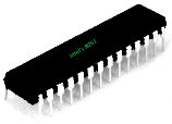
8051 Microcontroller
System on a Chip :
It is also referred to as System on a Chip (SoC) microcontroller because it is a chip circuit/integrated circuit that holds many components of a computer together on a single chip which include CPU, memory, input output ports(I/O ports), timers and secondary storage.
Features –
Some of the features include:-
16-byte bit-addressable RAM
Q2) Explain 8051 architecture?
A2)
Central Processor Unit (CPU)
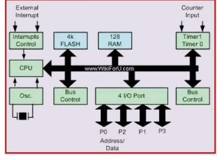
CPU is the brain of any processing device of the microcontroller. It monitors and controls all operations that are performed on the Microcontroller units. It reads program written in ROM memory and executes them and does the expected task of that application.
Interrupts
Interrupt is a subroutine call that interrupts the microcontrollers main operations or work and causes it to execute any other program, at the time of operation. An Interrupts gives us a mechanism to put on hold the ongoing operations, execute a subroutine and then again resumes to another type of operations.
Generally, five interrupt sources are there in 8051 Microcontroller.
(INT0) ̅ and (INT1) ̅ are external interrupts that could be negative edge triggered or low level triggered. When All these interrupts are activated, set the corresponding flags except for serial interrupt.
The interrupt flags are cleared when the processor branches to the interrupt service routine (ISR). The timers and serial port interrupts are external interrupts.
Memory
The program tells microcontroller to do specific tasks. These programs require a memory where they can be saved and read by Microcontroller to perform specific operations of a task.
The memory which is used to store the program known as code memory or Program memory It is also known as ROM memory.
The data memory of the 8051 is used to store data temporarily for operation is known RAM memory. 8051 microcontroller has 4K of code memory or program memory, that has 4KB ROM and also 128 bytes of data memory of RAM.
BUS
Basically, Bus is a collection of wires which work as a communication channel or medium for transfer of Data. These buses consist of 8, 16 or more wires of the microcontroller. Thus, these can carry 8 bits,16 bits simultaneously. Here two types of buses that are shown in below
Address Bus: Microcontroller 8051 has a 16 bit address bus for transferring the data. It is used to address memory locations and to transfer the address from CPU to Memory of the microcontroller. It has four addressing modes that are
Data Bus: Microcontroller 8051 has 8 bits of data bus, which is used to carry data of particular applications.
Oscillator
The 8051 microcontroller has an on-chip oscillator which works as a clock source for Central Processing Unit of the microcontroller. The output pulses of oscillator are stable. Therefore, it enables synchronized work of all parts of the 8051 Microcontroller.
Input/Output Port
Normally microcontroller is used in embedded systems to control the operation of machines in the microcontroller. Therefore, to connect to other machines, devices or peripherals we require I/O interfacing ports in the microcontroller interface. For this purpose, microcontroller 8051 has 4 input, output ports to connect it to the other peripherals
Timers/Counters
8051 microcontroller has two 16-bit timers and counters. These counters are again divided into 8-bit register. The timers are used for measurement of intervals to determine the pulse width of pulses.
Q3) Explain the memory organization?
Program Memory (ROM) of 8051
In 8051 Microcontroller, the code or instructions that must be executed are stored in the Program Memory, which is also called as the ROM of the Microcontroller. The original 8051 Microcontroller by Intel has 4KB of internal ROM.
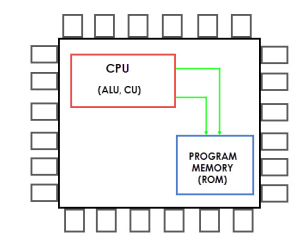
In 4KB of Internal ROM, the address space is 0000H to 0FFFH. If the address space that is the program addresses exceeds this value, then the CPU will automatically fetch the code from the external Program Memory.
For External Access Pin (EA Pin) must be pulled HIGH i.e. when the EA Pin is high, the CPU first fetches instructions from the Internal Program Memory in the address range of 0000H to 0FFFFH and if the memory addresses exceed the limit, then the instructions are fetched from the external ROM in the address range of 1000H to FFFFH.
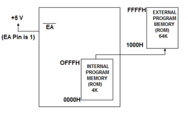
xternal access
There is also an alternative method to fetch the instructions that is ignore the Internal ROM and fetch all the instructions only from External Program Memory(External ROM).
For this purpose EA pin must be connected to GND . In this case the memory addresses of external ROM will be from 0000H to FFFFH.
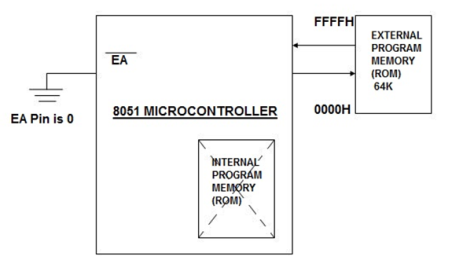
External Program Memory
Data Memory (RAM) of 8051 Microcontroller
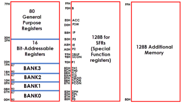
Lower 128B(00H to 07H) Upper 128B(80H-FFH)
(Direct and Indirect Addressing) (Direct Addressing) (Indirect Addressing)
Q5) Explain SFR?
A5) Register A/Accumulator
The Accumulator (sometimes referred to as Register A also) holds the result of most of arithmetic and logic operations. ACC is usually accessed by direct addressing and its physical address is E0H. Accumulator is both byte and bit addressable.

Register B
The major purpose of this register is in executing multiplication and division. The 8051 micro controller has a single instruction for multiplication (MUL) and division (DIV).
Ex: MUL A,B – When this instruction is executed, data inside A and data inside B is multiplied and answer is stored in A.
Note: For MUL and DIV instructions, it is necessary that the two operands must be in A and B.

Port Registers
4 Input/Output ports named P0, P1, P2 and P3 has got four corresponding port registers with same name P0, P1, P2 and P3. Data must be written into port registers first to send it out to any other external device through ports. Similarly any data received through ports must be read from port registers for performing any operation. All 4 port registers are bit as well as byte addressable.
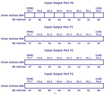
From the figure:-
Stack Pointer
Stack pointer is an 8 bit register, the direct address of SP is 81H and it is only byte addressable, which means you cant access individual bits of stack pointer. The content of the stack pointer points to the last stored location of system stack. To store something new in system stack, the SP must be incremented by 1 first and then execute the “store” command. Usually after a system reset SP is initialized as 07H and data can be stored to stack from 08H onwards.
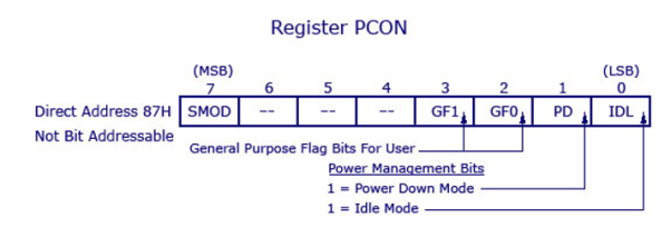
Setting bit 0 will move the micro controller to Idle mode and Setting bit 1 will move the micro controller to Power down mode.
Processor Status Word (PSW)
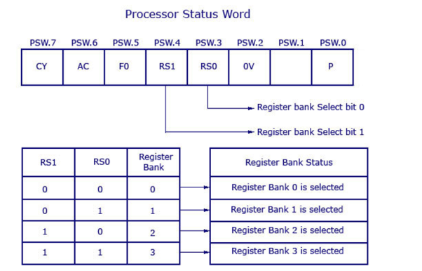
The picture below shows PSW register and the way register banks are selected using PSW register bits – RS1 and RS0. PSW register is both bit and byte addressable. The physical address of PSW starts from D0H. The individual bits are then accessed using D1, D2 … D7.
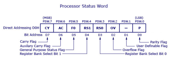
Bit No | Bit Symbol | Direct Address | Name | Function |
0 | P | D0 | Parity | This bit will be set if ACC has odd number of 1’s after an operation. If not, bit will remain cleared. |
1 | – | D1 |
| User definable bit |
2 | OV | D2 | Overflow | OV flag is set if there is a carry from bit 6 but not from bit 7 of an Arithmetic operation. It’s also set if there is a carry from bit 7 (but not from bit 6) of Acc |
3 | RS0 | D3 | Register Bank select bit 0 | LSB of the register bank select bit. Look for explanation below this table. |
4 | RS1 | D4 | Register Bank select bit 1 | MSB of the register bank select bits. |
5 | F0 | D5 | Flag 0 | User defined flag |
6 | AC | D6 | Auxiliary carry | This bit is set if data is coming out from bit 3 to bit 4 of Acc during an Arithmetic operation. |
7 | CY | D7 | Carry | Is set if data is coming out of bit 7 of Acc during an Arithmetic operation. |
There are 4 register banks named 0,1,2 and 3. Each bank has 8 registers named from R0 to R7. At a time only one register bank can be selected. Selection of register bank is made possible through PSW register bits PSW.3 and PSW.4, named as RS0 and RS1.These two bits are known as register bank select bits as they are used to select register banks.
SFR | Address | Function |
DPH | 83 | Data pointer registers (High). Only byte addressing possible. |
DPL | 82 | Data pointer register (Low). Only byte addressing possible. |
IP | B8 | Interrupt priority. Both bit addressing and byte addressing possible. |
IE | A8 | Interrupt enable. Both bit addressing and byte addressing possible. |
SBUF | 99 | Serial Input/Output buffer. Only byte addressing is possible. |
SCON | 98 | Serial communication control. Both bit addressing and byte addressing possible. |
TCON | 88 | Timer control. Both bit addressing and byte addressing possible. |
TH0 | 8C | Timer 0 counter (High). Only byte addressing is possible. |
TL0 | 8A | Timer 0 counter (Low). Only byte addressing is possible. |
TH1 | 8D | Timer 1 counter (High). Only byte addressing is possible. |
TL1 | 8B | Timer 1 counter (Low). Only byte addressing is possible. |
TMOD | 89 | Timer mode select. Only byte addressing is possible. |
Q6) Explain port operation?
A6)
PORT P0: When there is no external memory present, this port acts as a general-purpose input/output port. In the presence of external memory, it functions as a multiplexed address and data bus. It performs a dual role.
PORT P1: This port is used for various interfacing activities. This 8-bit port is a normal I/O port, does not perform dual functions.
PORT P2: Similar to PORT P0, this port can be used as a general purpose port when there is no external memory but when external memory is present it works in conjunction with PORT PO as an address bus. This is an 8-bit port and performs dual functions.
PORT P3:
Each port has 8 pins. Thus, the four ports jointly comprise 32 pins.
Features of Port 0
Functions of Port 0
Simple I/O port:
When we use Port 0 as an input port, the internal latch should know that it’s being used for input, and thus, a digital 1 (FFH) is written at the port address of 80H. This turns off the transistors causing the pin to float in high impedance state connecting it to the input buffer.
We can read data from ‘Read Pin Data’/’Read Latch Bit.’
When we use Port 0 as an output port, the latch programmed to 0 will turn on. Consequently, the FET will connect to GND. We will require an external pull up resistor(10k Ohm) here to give a logic ‘1’ for using Port 0 as an output port.
Access external memory:
When the 8051 wants to access external memory, the address for the memory generates due to Port 0 and Port 2. We get the lower half of the address from Port 0 and the upper half from Port 2. This is done using ALE pulses, which help to latch the address to the external bus. Once done, the Port 0 goes back to being an input port to read data from that memory.
Working of port 0
To configure port 0 as an input port the internal bus writes 1 to the D flip flop and the control pin is set to 0(Upper FET is OFF). The mux is connected to Q'(0) of the D flip flop as the control pin is 0. Due to this, the pin is connected to the input buffer which can be read to get the input data.
To use the port as an output port 0 is written to the D flip flop with the control signal being set to 0. This enables the lower FET and disables the upper FET due to this the pin gets connected to the ground and a zero is written to the output device.
To write a 1 to the external device the microcontroller writes 1 to the D flip flop which drives the pin to a high impedance state as it is not connected to either VCC or ground.
Features of Port 1:
The function of Port 1 – I/O port:
Features of Port 2
Functions of Port 2
I/O port:
It is quite similar to Port 0 The only difference here is that in Port 2, we use one FET with an internal pull-up resistor instead of the two FETs we saw in Port 0.
Memory Access:
Port 2 is used in conjunction with Port 0 to generate the upper address of the external memory location that needs to be accessed. However, one key difference is that it doesn’t need to turnaround and get a 1 in the latch immediately for input as in Port 0. It can remain stable.
What are the features and functions of Port 3 in 8051?
Features of Port 3
Functions of Port 3
I/O port
Just like Port 2, Port 3 can function as an input-output port.
Alternate SFR function
The input to SFR 1, we get the output of latch as 1, which turns on the NAND gate, and depending on the value of ‘Alternate Output Pin,’ FET will be wither ON/OFF.
P3 | Bit | Pin |
P3.0 | 0-RxD | 10 |
P3.1 | 1-TxD | 11 |
P3.2 | 2-INTO | 12 |
P3.3 | 3-INT1 | 13 |
P3.4 | 4-T0 | 14 |
P3.5 | 5-T1 | 15 |
P3.6 | 6-WR | 16 |
P3.7 | 7-RD | 17 |
RXD: this is used for a serial input port
TXD: this is used for serial output port
INT0: this used for an external interrupt 0
INT1: this used for external interrupt 1
T0: Timer 0 external input
T1: Timer 1 external input
WR: external data memory write strobe
RD: external data memory Read strobe
Q7) Explain memory interfacing?
A7) If external program/data memory are to be interfaced, they are interfaced in the following way.
External program memory is fetched if either of the following two conditions are satisfied.
1. (Enable Address) is low. The microcontroller by default starts searching for program from external program memory.
2. PC is higher than FFFH for 8051 or 1FFFH for 8052. tells the outside world whether the external memory fetched is program memory or data memory. is user configurable is processor controlled.
Q8) Explain programming 8051 resources?
A8) Each line or statement of the assembly language program of 8051 Microcontroller consists of three fields:
Label, Instruction and Comments.
The arrangement of these fields or the order in which they appear is shown below.
[ Label] Instructions [ // Comments]
TESTLABEL: MOV A,24H THIS IS SAMPLE COMMENT
In the above statement, the “TESTLABEL” is the name of the Label, “MOV A, 24H” is the Instruction and the “THIS IS A SAMPLE COMMENT” is a Comment.

Label
The Label is programmer chosen name for a Memory Location or a statement in a program. The Label part of the statement is optional and if present, the Label must be terminated with a Colon (:).
An important point to remember while selecting a name for the Label is that they should reduce the need for documentation.
Instruction
The Instruction is the main part of the 8051 Microcontroller Assembly Language Programming as it is responsible for the task performed by the Microcontroller. Any Instruction in the Assembly Language consists of two parts: Op-code and Operand(s).
Op -code Operand
MOV A,22H ; Move 22H to Accumulator
A – Destination
22H – source
The first part of the Instruction is the Op-code, which is short for Operation Code, specifies the operation to be performed by the Microcontroller. Op-codes in Assembly Language are called as Mnemonics.
Op-codes are in binary format (used in Machine Language) while the Mnemonic (which are equivalent to Op-codes) are English like statements.
The second part of the instruction is called the Operand(s) and it represents the Data on which the operation is performed.
There are two types of Operands: the Source Operand and the Destination Operand. The Source Operand is the Input of the operation and the Destination Operand is where the result is stored.
Q9) Write a short note on interrupts?
Each interrupt can be enabled or disabled by setting bits of the IE register. Likewise, the whole interrupt system can be disabled by clearing the EA bit of the same register.
As shown in the figure
The external interrupts – INT 0 and INT 1.
If the IT0 and IT1 bits of the TCON register are set, an interrupt will be generated on high to low transition, i.e. on the falling pulse edge (only in that moment).
If these bits are cleared, an interrupt will be continuously executed as far as the pins are held low.
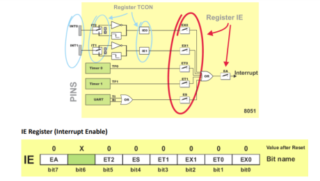
EA – global interrupt enable/disable:
o 0 – disables all interrupt requests.
o 1 – enables all individual interrupt requests.
ES – enables or disables serial interrupt:
o 0 – UART system cannot generate an interrupt.
o 1 – UART system enables an interrupt.
ET1 – bit enables or disables Timer 1 interrupt:
o 0 – Timer 1 cannot generate an interrupt.
o 1 – Timer 1 enables an interrupt.
EX1 – bit enables or disables external 1 interrupt:
o 0 – change of the pin INT0 logic state cannot generate an interrupt.
o 1 – enables an external interrupt on the pin INT0 state change.
ET0 – bit enables or disables timer 0 interrupt:
o 0 – Timer 0 cannot generate an interrupt.
o 1 – enables timer 0 interrupt.
EX0 – bit enables or disables external 0 interrupt:
o 0 – change of the INT1 pin logic state cannot generate an interrupt.
o 1 – enables an external interrupt on the pin INT1 state change.
If an interrupt of higher priority arrives while an interrupt is in progress, it will be immediately stopped and the higher priority interrupt will be executed first.
If two interrupt requests, at different priority levels, arrive at the same time then the higher priority interrupt is serviced first.
If both interrupt requests, at the same priority level, occur one after another, the one which came later has to wait until routine being in progress ends.
If two interrupt requests of equal priority arrive at the same time then the interrupt to be serviced is selected according to the following priority list:
1. External interrupt INT0
2. Timer 0 interrupt
3. External Interrupt INT1
4. Timer 1 interrupt
5. Serial Communication Interrupt IP Register (Interrupt Priority)
The IP register bits specify the priority level of each interrupt (high or low priority).

PS – Serial Port Interrupt priority bit
o Priority 0
o Priority 1
PT1 – Timer 1 interrupt priority
o Priority 0
o Priority 1
PX1 – External Interrupt INT1 priority
o Priority 0
o Priority 1
PT0 – Timer 0 Interrupt Priority
o Priority 0
o Priority 1
PX0 – External Interrupt INT0 Priority
o Priority 0
o Priority 1
When an interrupt request happens the following occurs:
1. Instruction in progress is ended.
2. The address of the next instruction to execute is pushed on the stack.
3. Depending on which interrupt is requested, one of 5 vectors (addresses) is written to the program counter in accordance to the table below:

These addresses store appropriate subroutines processing interrupts. Instead of them, there are usually jump instructions specifying locations on which these subroutines reside.
When an interrupt routine is executed, the address of the next instruction to execute is popped from the stack to the program counter and interrupted program resumes operation from where it left off.
Q10) Explain the programming model of 8051?
Directives (or pseudo-instructions) Give directions to the assembler. Assembling and running an 8051 program
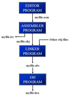
The step of Assembly language program are outlines as follows:
1) First, we use an editor to type a program for excellent editors or word processors are available that can be used to create and/or edit the program. Notice that the editor must be able to produce an ASCII file. For many assemblers, the file names follow the usual DOS conventions, but the source file has the extension “asm“ or “src”, depending on which assembly used.
2) The “asm” source file containing the program code created in step 1 is fed to an 8051assembler. The assembler converts the instructions into machine code.The assembler will produce an object file and a list file. The extension for the object file is “obj” while the extension for the list file is “lst”.
3) Assembler require a third step called linking. The linker program takes one or more object code files and produce an absolute object file with the extension “abs”. This abs file is used by 8051 trainers that have a monitor program.
4) Next the “abs” file is fed into a program called “OH” (object to hex converter) which creates a file with extension “hex” that is ready to burn into ROM.
Q11) Explain operand addressing?
A11) Register Direct Addressing Mode
In this addressing mode we use the register name directly (as source operand). An example is shown below.
MOV A, R4
S,o we see that opcode for MOV A, R4 is EC. The opcode is stored in program memory address 0202 and when it is executed the control goes directly to R4 of the respected register bank that is selected in PSW.
Register Indirect Addressing Mode
So, in this addressing mode, address of the data (source data to transfer) is given in the register operand.
MOV A, @R0
Here the value inside R0 is considered as an address, which holds the data to be transferred to accumulator.
Example: If R0 holds the value 20H, and we have a data 2F H stored at the address 20H, then the value 2FH will get transferred to accumulator after executing this instruction.
Indexed Addressing Mode
MOVC A, @A+DPTR and MOVC A, @A+PC
where DPTR is data pointer and PC is program counter (both are 16 bit registers).
Q12) Explain data transfer instructions?
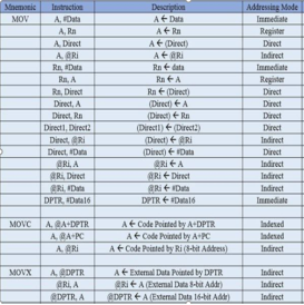
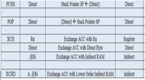
A12) The Data Transfer Instructions relate to transfer of data between registers or external program memory or data memory. The Mnemonics associated with Data Transfer are given below.
Q13) Explain arithmetic instructions?
The Mnemonics associated with the Arithmetic Instructions of the 8051 Microcontroller Instruction Set are:
The arithmetic instructions have no knowledge about the data format that is signed, unsigned, ASCII, BCD, and so on. The operations performed by the arithmetic instructions affect flags like carry, overflow, zero, etc. in PSW Register.
Mnemonic | Instruction | Description | Addressing Mode |
ADD | A,#data | A <- A + Data | Immediate |
| A,Rn | A<- A + Rn | Register |
| A,Direct | A<- A + (Direct) | Direct |
| A,@Ri | A<- A + @Ri | Indirect |
|
|
|
|
ADDC | A,#data | A <- A + Data + C | Immediate |
| A,Rn | A<- A + Rn + C | Register |
| A,Direct | A<- A + (Direct)+C | Direct |
| A,@Ri | A<- A + @Ri +C | Indirect |
|
|
|
|
SUBB | A,#data | A <- A – Data | Immediate |
| A,Rn | A<- A- Rn | Register |
| A,Direct | A<- A - (Direct) | Direct |
| A,@Ri | A<- A XRL-Ri | Indirect |
|
|
|
|
MUL AB | Multiply A with B |
|
|
|
|
|
|
DIV AB | Divide A by B |
|
|
|
|
|
|
DEC A | A,#data | A <- A -1 |
|
| A,Rn | Rn <-Rn -1 |
|
| A,Direct | (Direct) <- (Direct) -1 |
|
| A,@Ri | @Ri<- @Ri -1 |
|
INC A | A,#data | A <- A+1 |
|
| A,Rn | Rn <-Rn +1 |
|
| A,Direct | (Direct)<- (Direct) +1 |
|
| A,@Ri | @Ri<- @Ri+1 |
|
DA | A | Decimal Adjust Accumulator |
|
Q14) Explain logic instructions?
Mnemonics associated with Logical Instructions are as follows:
Mnemonic | Instruction | Description | Addressing Mode |
ANL | A,#data | A <- A AND Data | Immediate |
| A,Rn | A<- A AND Rn | Register |
| A,Direct | A<- A AND (Direct) | Direct |
| A,@Ri | A<- A AND @Ri | Indirect |
| Direct A | (Direct ) <- (Direct ) AND A | Direct |
| Direct , # Data | (Direct ) <- (Direct ) AND # Data | Direct |
|
|
|
|
ORL | A,#data | A <- A OR Data | Immediate |
| A,Rn | A<- A OR Rn | Register |
| A,Direct | A<- A OR (Direct) | Direct |
| A,@Ri | A<- A OR @Ri | Indirect |
| Direct A | (Direct ) <- (Direct ) OR A | Direct |
| Direct , # Data | (Direct ) <- (Direct ) OR # Data | Direct |
|
|
|
|
XRL | A,#data | A <- A XRL Data | Immediate |
| A,Rn | A<- A XRL Rn | Register |
| A,Direct | A<- A XRL (Direct) | Direct |
| A,@Ri | A<- A XRL @Ri | Indirect |
| Direct A | (Direct ) <- (Direct ) XRL A | Direct |
| Direct , # Data | (Direct ) <- (Direct ) XRL # Data | Direct |
|
|
|
|
CLR | A | A<-00H |
|
CPL | A | A<-A |
|
|
|
|
|
RL | A | Rotate ACC Left |
|
|
|
|
|
RLC | A | Rotate ACC Left through carry |
|
RR | A | Rotate ACC right |
|
|
|
|
|
RRC | A | Rotate ACC right through carry |
|
SWAP | A | Swap nibbles within ACC |
|
Q15) Explain control transfer instructions?
A15)
JZ label ; Jump if A=0
JNZ label ; Jump if A!=0
DJNZ reg, label ; Decrement and Jump if A (or reg.) !=0
CJNE A, byte ; Compare and Jump if A!=byte
CJNE reg, #data ; Compare and Jump if byte!=data
JC ; Jump if Carry=1 J
NC ; Jump if Carry=0
JB ; Jump if bit =1
JNB ; Jump if bit =0
JBC ; Jump if bit=1 and clear bit
LCALL: 3-byte instruction • When subroutine is called – Control is transferred to that subroutine – Processor saves the PC onto the Stack and begins to fetch instructions from new location. – RET (return to caller) POP from Stack to PC.
ACALL:
2-byte instruction
• ACALL’s target address must be with in a 2KB range
Q16) Explain the programming of 8051?
A16) The 8051 Microcontroller Assembly Language Program will start assembling from the Program Memory Address 0000H. This is also the address from which the 8051 Microcontroller will start executing the code.
In order place the Program and Data anywhere in the Address Space of the 8051 Microcontroller, you can use the ORG Directive.
Examples
ORG 0000H ; Tells the Assembler to assemble the next statement at 0000H
LJMP MAIN ; Code Memory at 0000H. Jump to MAIN.
ORG 000BH ; Tells the Assembler to assemble the next statement at 000BH
MAIN: NOP ; Code Memory at 000BH. MAIN starts here.
DB – Define Byte
The DB Directive is used to define a Byte type variable. Using this directive, you can define data in Decimal, Binary, HEX or ASCII formats. There should be a suffix of ‘B’ for binary and ‘H’ for HEX. The ASCII Characters are placed in single quotation marks (like ‘string’).
Examples
ORG 0000H
DB 10 ; Define Byte 10 (Decimal) and store at 0000H
DB 30H ; Define Byte 30 (HEX) and store at 0001H
DB ‘STRING’ ; Define String ‘STRING’ and store at 0002H to 0007H
DB 00001111B ; Define Byte 00001111 (Binary) and store at 0008H
DB 1234H ; Define Byte 34 (HEX) and store at 0009H. Only lower byte is
accepted as DB can allocate only a Byte of Memory.
DW – Define Word
The Define Word (DW) Directive is used to include a 16-bit data in a program. The functionality of DW is similar to that of DB except that DW generates 16-bit values.
EQU – Equate
Using the EQU Directive, you can associate a Symbol (or Label) with a Value.
Examples
TMP EQU #30 ; Assigns the value #30 to the name TMP
RED_LED EQU P1.0 ; P1.0 is defined as RED_LED
END
The END Directive is used to stop the assembling process. This should be the last statement in the program. END Directive cannot have a Label and the statements beyond END will not be processed by the Assembler.
Example
ORG 0000H
MOV A, 20H
MOV R0, #30
END
The following is a simple Assembly Language for 8051 Microcontroller which copies the data from R0 of Bank0 to R0 of Bank3.
ORG 00H
MOV R0, #33H
MOV A, R0
SETB PSW.3
SETB PSW.4
MOV R0, A
END