Unit - 5
8086
Q1) Explain maximum mode configuration?
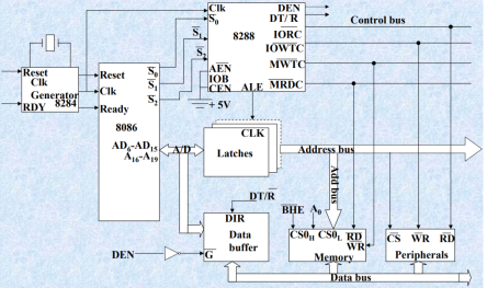
A1) In the maximum mode, there may be more than one microprocessor in the system configuration.
• The components in the system are same as in the minimum mode system.The basic function of the bus controller chip IC8288, is to derive control signals like RD and WR ( for memory and I/O devices), DEN, DT/R, ALE etc. using the information by the processor on the status lines.
• The bus controller chip has input lines S 2, S1, S 0 and CLK. These inputs to 8288 are driven by CPU.
• It derives the outputs ALE, DEN, DT/R, MRDC, MWTC, AMWC, IORC, IOWC and AIOWC. The AEN, IOB and CEN pins are specially useful for multiprocessor systems.AEN and IOB are generally grounded. CEN pin is usually tied to +5V. The significance of the MCE/PDEN output depends upon the status of the IOB pin.
• If IOB is grounded, it acts as master cascade enable to control cascade 8259A, else it acts as peripheral data enable used in the multiple bus configurations. • INTA pin used to issue two interrupt acknowledge pulses to the interrupt controller or to an interrupting device.IORC, IOWC are I/O read command and I/O write command signals respectively . These signals enable an IO interface to read or write the data from or to the address port.
• The MRDC, MWTC are memory read command and memory write command signals respectively and may be used as memory read or write signals.
• All these command signals instructs the memory to accept or send data from or to the bus.
• For both of these write command signals, the advanced signals namely AIOWC and AMWTC are available.
The maximum mode system timing diagrams are divided in two portions as read (input) and write (output) timing diagrams.
• The address/data and address/status timings are similar to the minimum mode.
• ALE is asserted in T1, just like minimum mode. The only difference lies in the status signal used and the available control and advanced command signals.
Q2) Explain DMA?
A2) The direct memory access (DMA) I/O technique provides direct access to the memory while the microprocessor is temporarily disabled.
• A DMA controller temporarily borrows the address bus, data bus, and control bus from the microprocessor and transfers the data bytes directly between an I/O port and a series of memory locations.
• The DMA transfer is also used to do high-speed memory-tomemory transfers. • Two control signals are used to request and acknowledge a DMA transfer in the microprocessor-based system.
• The HOLD signal is a bus request signal which asks the microprocessor to release control of the buses after the current bus cycle.
• The HLDA signal is a bus grant signal which indicates that the microprocessor has indeed released control of its buses by placing the buses at their high-impedance states.
• The HOLD input has a higher priority than the INTR or NMI interrupt inputs.
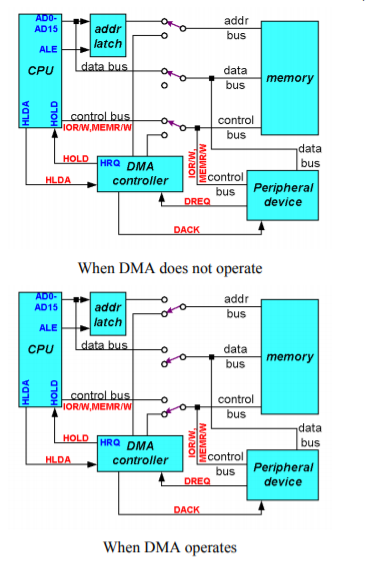
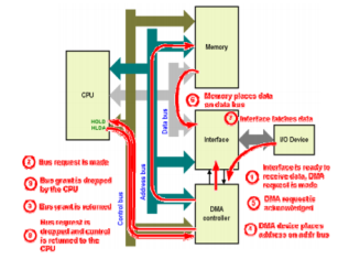
Figure. Memory to device transfer.
Q3) Explain Dto A interfacing?
A3) The Digital to Analog Converters (DAC) convert binary numbers into their analog equivalent voltages.
The DAC find applications in areas like
Digitally controlled gains
Motor speed controls
Programmable gain amplifiers etc.
AD 7523 8-Bit Multiplying DAC:--
• Intersil’s AD 7523 is a 16 pin DIP, multiplying digital to analog converter, containing R-2R ladder (R=10K) for digital to analog conversion.
✓ Power supply +5v to +15v
✓ Vref -> -10v to +10v
✓ The maximum analog output voltage will be +10v
✓ A Zener is connected between OUT1 & OUT2 to save the DAC from negative transients.
✓An operational amplifier is used as a current – to – voltage converter at the output of AD 7523.
✓An external feedback resister acts to control the gain.
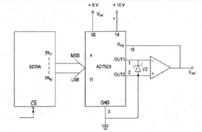
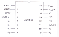
Problem:-- Interface DAC AD7523 with the 8086 running at 8MHz & write ALP to generate a saw tooth waveform of period 1ms with Vmax 5v.
Solution:--
Code segment
Assume cs:code
Start: MOV AL, 80H
OUT CWR, AL
AGAIN: MOV AL, 00H
BACK: OUT Port A, AL
INC AL
CMP AL, 0F2H
JB BACK
JMP AGAIN
Code ends
End Start
Q4) Explain A to D converter?
A4) The time taken by the ADC from the active edge of SOC pulse till the active edge of EOC signal is called as the conversion delay of the ADC.
General algorithm for ADC interfacing contains the following steps
The analog to digital converter chips 0808 and 0809 are 8- bit CMOS, successive approximation converters. It is fastest technique.
The conversion delay is 100 µs at a clock frequency of 640 kHz, which is quite low as compared to other converters. Block Diagram of ADC 0808/0809 This converter internally has a 3:8 analog multiplexer, so that at a time 8 different analog inputs can be connected to the chips. Out of these 8 inputs only one can be selected for conversion by using 3 address lines A,B,C. The CPU may drive these lines using output port lines in case of multichannel applications.
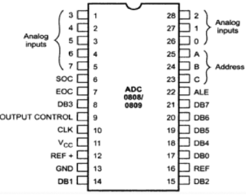
Analog input selected | C | B | A |
i/p 0 | 0 | 0 | 0 |
i/p 1 | 0 | 0 | 1 |
i/p 2 | 0 | 1 | 0 |
i/p 3 | 0 | 1 | 1 |
i/p 4 | 1 | 0 | 0 |
i/p 5 | 1 | 0 | 1 |
i/p 6 | 1 | 1 | 0 |
i/p 7 | 1 | 1 | 1 |
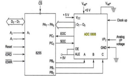
Q5) Interface ADC 0808 with 8086 using 8255 ports. Use Port A of 8255 for transferring digital data output of ADC to the CPU & Port C for control signals. Assume that an analog input is present at I/P2 of the ADC and a clock input of suitable frequency is available for ADC. Draw the schematic & timing diagram of different signals of ADC0808.
A5) •The analog input I/P2 is used & therefore address pins A,B,C should be 0,1,0 respectively to select I/P2.
•The OE (Out put latch Enable) & ALE pins are already kept at +5v to select the ADC and enable the outputs.
•Port C upper acts as the input port to receive the EOC signal while Port C lower acts as the output port to send SOC to ADC.
•Port A acts as a 8-bit input data port to receive the digital data output from the ADC.
8255 Control Word:
D7 D6 D5 D4 D3 D2 D1 D0
1 0 0 1 1 0 0 0 = 98H
Program:
MOV AL,98H ; Initialize 8255, send AL to control word (CWR)
OUT CWR, AL
MOV AL, 02H ;Select I/P2 as analog I/P
OUT Port B, AL ;Port B as output
MOV AL, 00H ; Give start of conversion pulse to the ADC
OUT Port C, AL
MOV AL, 01H
OUT Port C, AL
MOV AL, 00H
OUT Port C, AL
WAIT: IN AL, Port C ; check for EOC by reading Port C upper & rotating RCL ; through carry.
JNC WAIT IN AL, Port A ; if EOC, read digital equivalent in AC
HLT ; stop.
Q6) Explain CRT terminal ?
A6) The CRT terminal looks like television with type writer like keyboard. It allows the programmer to enter programs and data to computerdirectly to the computer.
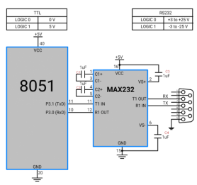
The CRT terminal uses RS 232 interface for communication with microprocessor.
3 signals in the RS-232C are TX,RX,GND are used for interfacing CRT terminal with microprocessor.
TXD is used for transmission of data from CRT to the microprocessor
RXD is used for receiving data from miroprocessor into the CRT
GND signal in the CRT is connected to the GND signal in the microprocessor
RS-232 interface transmits or receives the data by serial communication that is one bit of data is transmitted or recived by RS-232 C interface at a time.
Each byte of data is transmitted or recived by Rs-232 inrerface enclosed by one start bit and 1,1.5 and 2 stop bits.
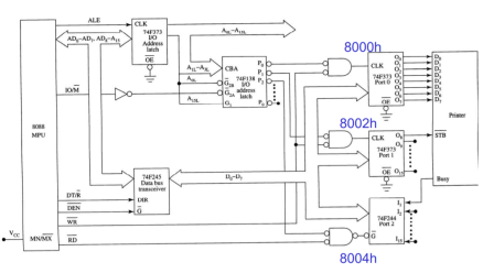
Q7) Explain Printer interface?
A7)
Q8) Explain programming of 8051 timers?
A8) In Intel 8051, there are two 16-bit timer registers. These registers are known as Timer0 andTimer1. The timer registers can be used in two modes. These modes are Timer mode and the Counter mode. The only difference between these two modes is the source for incrementing the timer registers.
Timer Mode
In the timer mode, the internal machine cycles are counted. So this register is incremented in each machine cycle. So when the clock frequency is 12MHz, then the timer register is incremented in each millisecond. In this mode it ignores the external timer input pin.
Counter Mode
2 are for both of the Timer/Counter. Mode 3 has a different meaning for each timer register. There is a register called TMOD. This register can be programmed to configure these timers or counters.
Timer | Timer1 Mode | Timer0 Mode | ||||||
Bit Details | Gate (G) | C/T | M1 | M0 | Gate (G) | C/T | M1 | M0 |
TMOD Register
TMOD(Timer Mode) is an SFR. The address of this register is 89H. This is not bit-addressable.
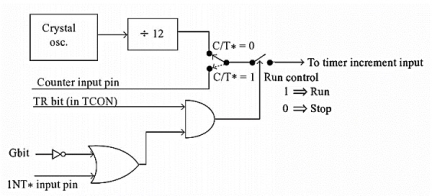
The circuit that controls the running of the timers is shown in the figure.
Bit Details | High Value(1) | Low Value(0) |
C/T | Configure for the Counter operations | Configure for the Timer operations |
Gate (G) | Timer0 or Timer1 will be in RunMode when TRX bit of TCON register is high. | Timer0 or Timer1 will be in RunMode when TRX bit of TCON register is high and INT0 or INT1 is high. |
Bit Details | 00 | 01 | 10 | 11 |
M1 M0 | This is for Mode 0. (8-bit timer/counter, with 5-bit pre-scaler) | This is Mode 1. (16-bit timer/counter) | This is Mode 3 (8-bit auto reload-timer/counter) | This is Mode 3 (The function depends on Timer0 or Timer1) |
The Gate bit will be high when the timer or counter is in mode 0 to 2.
Examples
To configure Timer0 as 16-bit event counter and Timer1 as 8-bit auto reload counter, use the bit pattern as 0 0 1 0 0 1 0 1. It is equivalent to 25H. Then if we want to program the TMOD register with this bit pattern, we can use this instruction:
MOVTMOD,#25H
The above instruction is executed, then the timer/counter will be controlled by the software. To configure the system as hardware controlled mode, then the gate bits will be 1. So the bit patterns will be 1 0 1 0 1 1 0 1 = ADH
Then use this instruction:
MOVTMOD,#0ADH
Mode 0 of Timer/Counter
The Mode 0 operation is the 8-bit timer or counter with a 5-bit pre-scaler. So it is a 13-bit timer/counter. It uses 5 bits of TL0 or TL1 and all of the 8-bits of TH0 or TH1.

In this example the Timer1is selected, in this case, every 32 (25)event for counter operations or 32 machine cycles for timer operation, the TH1 register will be incremented by 1. When the TH1overflows from FFH to 00H, then the TF1 of TCON register will be high, and it stops the timer/counter.
Example, we can say that if the TH1 is holding F0H, and it is in timer mode, then T
F1will be high after 10H * 32 = 512 machine cycles.
MOVTMOD,#00H
MOV TH1,#0F0H
MOV IE,#88H
SETB TR1
In the above program, the Timer1 is configured as timer mode 0. In this case Gate = 0. Then the TH1 will be loaded with F0H, then enable the Timer1 interrupt. At last set the TR1 of TCON register, and start the timer.
Mode 1 of Timer/Counter
The Mode 1 operation is the 16-bit timer or counter. In the following diagram, we are using Mode 1 for Timer0.

In this case every event for counter operations or machine cycles for timer operation, the TH0– TL0 register-pair will be incremented by 1. When the register pair overflows from FFFFH to 0000H, then the TF0 of TCON register will be high, and it stops the timer/counter.
Example, we can say that if the TH0 – TL0 register pair is holding FFF0H, and it is in timer mode, then TF0 will be high after 10H = 16 machine cycles. When the clock frequency is 12MHz, then the following instructions generate an interrupt 16 µs after Timer0 starts running.
MOV TMOD,#01H
MOV TLO,#F0H
MOV TH0, #0FFH
MOV IE,#82H
SETB TR0
In the above program, the Timer0 is configured as timer mode 1. In this case Gate = 0. Then the TL0 will be loaded with F0H and TH0 is loaded with FFH, then enable the Timer0 interrupt. At last set the TR0 of TCON register, and start the timer.
Mode 2 of Timer/Counter
The Mode 2 operation is the 8-bit auto reload timer or counter. In the following diagram, we are using Mode 2 for Timer1.
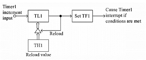
In this case every event for counter operations or machine cycles for timer operation, the TL1register will be incremented by 1. When the register pair overflows from FFH to 00H, then the TF1 of TCON register will be high, also theTL1 will be reloaded with the content of TH1 and starts the operation again.
Example, If the TH1 and TL1 register both are holding F0H and it is in timer mode, then TF1 will be high after 10H= 16 machine cycles. When the clock frequency is 12MHz this happens after 16 µs, then the following instructions generate an interrupt once every 16 µs after Timer1 starts running
MOV TMOD,#20H
MOV TL1,#0F0H
MOV TH1,#0F0H
MOV #88H
SETBTR1
In the above program, the Timer1 is configured as timer mode 2. In this case Gate = 0. Then the TL1 and TH1 are loaded with F0H. then enable the Timer1 interrupt. At last set the TR1 of TCON register, and start the timer.
Timer1 in mode 2 generates the desired baud rate when the serial port is working on Mode 1 or 3.
Programming of Counters and Timers:
In order to program 8051 timers, it is important to know the calculation of initial count value to be stored in the timer register.
The calculations are as follows. In any mode,
Timer Clock period = 1/Timer Clock Frequency. = 1/(Master Clock Frequency/12)
Upon starting the timer this value from THx will be reloaded to TLx register. (256D = FFH+1)
Steps for programming timers in 8051
Mode 1:
Load the TMOD value register indicating which timer (0 or 1) is to be used and which timer mode is selected. Load registers TL and TH with initial count values.
Stop the timer with the instructions “CLR TR0” or “CLR TR1”, for timer 0 and timer 1, respectively.
Clear the TF flag for the next round with the instruction “CLR TF0” or “CLR TF1”, for timer 0 and timer 1, respectively.
Go back to step 2 to load TH and TL again.
Mode 0: The programming techniques mentioned here are also applicable to counter/timer mode 0. The only difference is in the number of bits of the initialization value.
Mode 2:
Load the TMOD value register indicating which timer (0 or 1) is to be used; select timer mode
Load TH register with the initial count value. As it is an 8-bit timer, the valid range is from 00 to FFH.
Start the timer. Keep monitoring the timer flag (TFx) with the “JNB TFx,target” instruction to see if it is raised.
Get out of the loop when TFx goes high. Clear the TFx flag.
Go back to step 4, since mode 2 is auto-reload.
Q9) Write a program to continuously generate a square wave of 2 kHz frequency on pin P1.5 using timer 1. Assume the crystal oscillator frequency to be 12 MHz. s.s.
A9) Each half pulse = 250 The period of the square wave is T = 1/(2 kHz) = 500 s = 250s /1 s is: 250
The value n for 250 65536 - 250 = FF06H. TL = 06H and TH = 0FFH.
MOV TMOD,#10 ;Timer 1, mode 1
AGAIN: MOV TL1,#06H ;TL0 = 06H
MOV TH1,#0FFH ;TH0 = FFH
SETB TR1 ;Start timer 1
BACK: JNB TF1,BACK ;Stay until timer rolls over
CLR TR1 ;Stop timer 1
CPL P1.5 ;Complement P1.5 to get Hi, Lo
CLR TF1 ;Clear timer flag 1
SJMP AGAIN ;Reload timer
Q10) Explain 8051 serial interface?
Figure .Interface standard
Q11) Explain 80386 microprocessor?
A11) 80386 microprocessors was designed by Intel in October 1985 which is an upgraded version of 80286 microprocessor. It is a 32-bit processor that can carry out 32-bit operation in one cycle. It has data and address bus of 32-bit each.
The figure below shows the architectural representation of 80386 microprocessor:
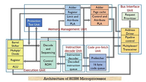
Basically it has 6 functional units which are as follows:
As we have already discussed that the 80386 possess the ability of 3 stage pipelining thus performs fetching, decoding and execution simultaneously along with memory management and bus accessing. Thus all these units operate parallely.
This pipelining technique leads to reduction in overall processing time thereby increasing the performance of the overall system.
Let us now move further and understand the operation of each unit in detail.
1. Bus Interface Unit
The bus interface unit or BIU holds a 32-bit bidirectional data bus as well as 32-bit address bus. Whenever a need for an instruction or a data fetch is generated by the system then the BIU generates signals (according to the priority) for activating the data and address bus in order to fetch the data from the desired address.
The BIU connects the peripheral devices through the memory unit and also controls the interfacing of external buses with the coprocessors.
2. Code Prefetch Unit
This unit fetches the instructions stored in the memory by making use of system buses. Whenever the system generates a need for an instruction then the code prefetch unit fetches that instruction from the memory and stores it in 16-byte prefetch queue.
So to speed up the operation this unit fetches the instructions in advance and the queue stores these instructions.
The sequence in which the instructions are fetched and gets stored in the queue depends on the order they exist in the memory.
As this unit fetches one double word in single access. So, in such a case, it is not necessary that each time only a single instruction will be fetched, as the fetched instruction can be parts of two different instructions.
It is to be noted here that, code prefetching holds lower priority than data transferring. As whenever, a need for data transfer is generated by the system then immediately the code prefetcher leaves the control over the buses. So that the BIU can transfer the required data.
But prefetching of instruction and storing it in the queue reduces the wait for the upcoming instruction to almost zero.
3. Instruction Decode Unit
We know that instructions in the memory are stored in the form of bits. So, this unit decodes the instructions stored in the prefetch queue. Basically the decoder changes the machine language code into assembly language and transfers it to the processor for further execution.
4. Execution Unit
The decoded instructions are stored in the decoded instruction queue. So, these instructions are provided to the execution unit in order to execute the instructions.
The execution unit controls the execution of the decoded instructions. This unit has a 32-bit ALU, that performs the operation over 32-bit data in one cycle. Also, it consists of 8 general purpose as well as 8 special purpose registers. These are used for data handling and calculation of offset address.
5. Memory Management Unit
This unit has two separate units within it. These are
Segmentation unit: The segmentation unit plays a vital role in the 80836 microprocessor. It offers protection mechanism in order to protect the code or data present in the memory from application programs.
It gives 4 level protection to the data or code present in the memory. Every information in the memory is assigned a privilege level from PL0 to PL3. Here, PL0 holds the highest priority and PL3 holds the lowest priority.
Suppose a file (either data or code) is needed to be accessed is stored in the memory at PL0. Then only those programs which are working at PL0 would be able to access that file. While other programs will not be able to access the same.
Also, if a file is present at PL1, then programs of PL0 and PL1 both can access it. As PL0 has higher priority than PL1. So, for protection purpose the main part of OS is stored in PL0 while PL3 holds the user programs.
Providing protection to the data or code inside the system is the most advantageous factor that was first given by 80386 microprocessor.
Paging Unit: The paging unit operates only in protected mode and it changes the linear address into physical address. As the programmer only provides the virtual address and not the physical address.
The segmentation unit controls the action of paging unit, as the segmentation unit has the ability to convert logical address into linear address at the time of executing an instruction.
Basically it changes the overall task map into pages and each page has a size of 4K. This allows the handling of task in the form of pages rather than segments.
Paging unit supports multitasking. This is so because the physical memory is not required to hold the whole segment of any task. Despite, only that part of the segment which is needed to be currently executed must be stored in that memory whose physical address is calculated by the paging unit.
This resultantly reduces the memory requirement and hence this frees the memory for other tasks. Thus,we get an effective way for managing the memory to support multitasking.
Q12) Explain 80486?
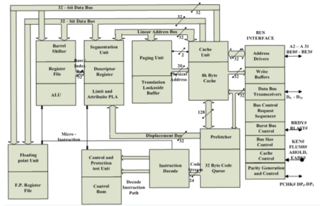
A12) The 32-bit 80486 is the next evolutionary step up from the 80386.
•One of the most obvious feature included in a 80486 is a built in math coprocessor.
This coprocessor is essentially the same as the 80387 processor used with a 80386, but being integrated on the chip allows it to execute math instructions about three times as fast as a 80386/387 combination.
•80486 is an 8Kbyte code and data cache.
•To make room for the additional signals, the 80486 is packaged in a 168 pin, pin grid array package instead of the 132 pin PGA used for the 80386.
Pin Definitions
•A 31-A2 : Address outputs A31-A2 provide the memory and I/O with the address during normal operation. During a cache line invalidation A31-A4 are used to drive the microprocessor.
•A20M3 : The address bit 20 mask causes the 80486 to wrap its address around from location 000FFFFFH to 00000000H as in 8086. This provides a memory system that functions like the 1M byte real memory system in the 8086 processors.
• ADS : The address data strobe become logic zero to indicate that the address bus contains a valid memory address.
•AHOLD: The address hold input causes the microprocessor to place its address bus connections at their high-impedance state, with the remainder of the buses staying active. It is often used by another bus master to gain access for a cache invalidation cycle.
•BREQ: This bus request output indicates that the 486 has generated an internal bus request.
• BE - BE 3 0 : Byte enable outputs select a bank of the memory system when information is transferred between the microprocessor and its memory and I/O. The BE3 signal enables D31 – D24 , BE2 enables D23-D16, BE1 enables D15 – D8 and BE0 enables D7-D0.
•BLAST: The burst last output shows that the burst bus cycle is complete on the next activation of BRDY# signal.
•BOFF : The Back-off input causes the microprocessor to place its buses at their high impedance state during the next cycle. The microprocessor remains in the bus hold state until the BOFF# pin is placed at a logic 1 level.
•NMI : The non-maskable interrupt input requests a type 2 interrupt.
•BRDY : The burst ready input is used to signal the microprocessor that a burst cycle is complete.
•KEN : The cache enable input causes the current bus to be stored in the internal. •LOCK : The lock output becomes a logic 0 for any instruction that is prefixed with the lock prefix.
•W / R : current bus cycle is either a read or a write.
•IGNNE : The ignore numeric error input causes the coprocessor to ignore floating point error and to continue processing data. The signal does not affect the state of the FERR pin.
•FLUSH : The cache flush input forces the microprocessor to erase the contents of its 8K byte internal cache.
•EADS : The external address strobe input is used with AHOLD to signal that an external address is used to perform a cache invalidation cycle.
•FERR : The floating point error output indicates that the floating point coprocessor has detected an error condition. It is used to maintain compatibility with DOS software.
•BS8 : The bus size 8, input causes the 80486 to structure itself with an 8-bit data bus to access byte-wide memory and I/O components.
•BS16 : The bus size 16, input causes the 80486 to structure itself with an 16-bit data bus to access word-wide memory and I/O components.
•PCHK : The parity check output indicates that a parity error was detected during a read operation on the DP3 – DP0 pin.
•PLOCK : The pseudo-lock output indicates that current operation requires more than one bus cycle to perform.
This signal becomes a logic 0 for arithmetic coprocessor operations that access 64 or 80 bit memory data.
