Module 01
Introduction to Semiconductors
A :- v=A Characteristic for forward bias:-
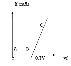
V-I Characteristics:-
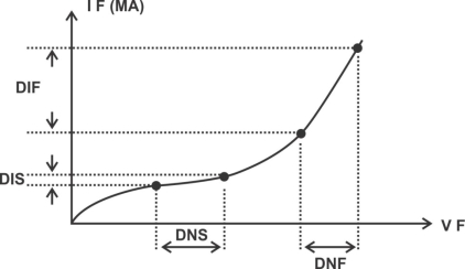
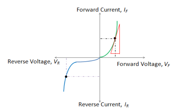
Graph shows how the dynamic resistance decrease as we move up the curve xd= DNF/DIF=
As we continue to increase the forward bias voltage the current continues to increase very rapidly ,but the voltage across the diode increase only gradually above 0.7 v.
This small increase in the diode vtg above the barrier potential is due to the voltage drop across the internal dynamic resistance of the semi conductive material.
Dynamic resistance:- A Resistance change as move along a V-I curve it is called dynamic or A. C resistance.
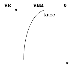
B) V - I Characteristics for Reverse biased :-

When the applied bias voltage is increased to a value where. the reverse vtg across the diode the reaches appropriately 0.7 v (barrier potential) the forward current begins to increase rapidly.
As we continue to increase the bias voltage the current continues to increase very rapidly bit the voltage across the diode increases very little above VBR.
IR increases little above VBR. resulting in overheating & possible damage.
2. Write short note on AC and DC Resistance of Diode.
Static or DC Resistance
It is the resistance offered by the diode to the flow of DC through it when we apply a DC voltage to it. Mathematically the static resistance is expressed as the ratio of DC voltage applied across the diode terminals to the DC flowing through it (shown by the black dotted line in Figure) i.e.
Dynamic or AC Resistance
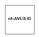
It is the resistance offered by the diode to the flow of AC through it when we connect it in a circuit which has an AC voltage source as an active circuit element. Mathematically the dynamic resistance is given as the ratio of change in voltage applied across the diode to the resulting change in the current flowing through it. This is shown by the slope-indicating red solid lines in Figure and is expressed as


3. Write and explain with example the Diode Current Equation.
 ampers
Where ,
V= Applied voltage across the diode in volts
I=Current flow through the diode in amperes.
n= 2 for silicon P-N junction diode
=1 for germanium P-N junction diode.
IO = reverse saturation current flow through diode in amperes.
VT =Is the voltage equivalent of temperature in volts.
VT= K X T volt’s
K=Boltzmann's constant
K=8.62 * 10 -s ev/k
I= temperature in ok
The equation VI= K * T indicates that the current flow through the diode also depend upon the ambient temperature.
Room temperature =25 0c
T= 273+25=298K
VT=K * T

4. Define: Avalanche breakdown and Zener Breakdown.
i) Avalanche breakdown:-As the magnitude of the reverse bias vtg is increased the kinetic energy of the minority carriers gets increased. while travelling the minority carriers collide with the stationery atoms which in turns results in breaking some of the covalent bond & generating free e- (carrier multiplication)
This process continues leading to a very swift multiplication giving rise to a large reverse current in just a few picoseconds. this effect is called as avalanche breakdown effect.
ii) Zener Breakdown: - This type of breakdown occurs in heavily doped P-N junction in which the depletion region is very narrow.
All the applied reverse voltage appears across the depletion layer. the electric field is vtg per unit distance. it is very intense at the depletion region.
There for it can pull the electronic out of the valance bond by breaking the covalent bonds and producing the free electrons. This process is known as zener effect.
Due to this heavy current flow & diode may damage.
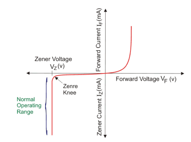
5. Draw and explain Zener Diode in detail.
PRINCIPLE OF OPERATION: - A zener diode can be forward biased or reverses biased. its operation in the forward biased mode is same as that of a p-n junction diode but its operation in the reverse biased mode is sustainably deferent.


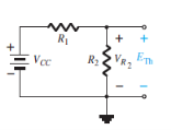
6. A 5.0V stabilized power supply is required to be produced from a 12V DC power supply input source. The maximum power rating PZ of the zener diode is 2W. Using the zener regulator circuit above calculate:
a). The maximum current flowing through the zener diode.
Maximum current = Watts/ Voltage =2W/5V =400mA
b). The minimum value of the series resistor, RS
 = 17.5 Ω
c). The load current IL if a load resistor of 1kΩ is connected across the zener diode.

d). The zener current IZ at full load.
Iz =Is -Il =440mA – 5mA = 395mA
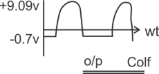
7. What would you expect to see displayed on oscilloscope connected across RL in the Limiter.

The diode is forward biased and conducts when then the i/p vtg goes below -0.7v so for the –ve limiter , the peak o/p vtg across RL can be determined by the following
Equation -
Volt =(RL/R+RL) Vin
=(1k/100+1k)10v
= 1K/1.1K*10
=1*103/1.1*103*10
= 1*104/11*102*10
= 1*104*10-2*10
=10/11 10*10*10/11
Volt = 10000/11 = 9.09V
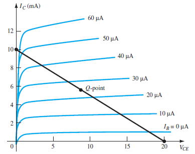
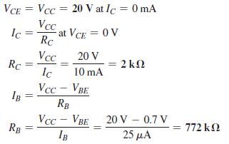
8. Determine the values of VCC RC and RB of a fixed bias configuration for a given load line and defined Q point.
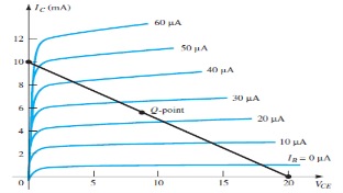
Solution:
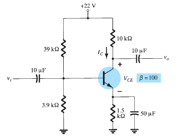
9. Determine dc bias voltage VCE and current IC for voltage divider configuration. (Ref. 2)
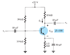
Solution:
