Unit - 4
Feedback amplifier and Oscillators
Q1) Determine the input power, output power and efficiency resulting in a class B push-pull amplifier providing a signal 20V peak to a 16 Ω load, using a single supply of VCC = 30V.
A1) Given: VL(p) = 20 V, RL = 16 Ω, VCC = 30 V
The input power is given by,
Pi(dc) = VCC(2 / ∏ I / p) = VCC.2 / ∏.VL(p) / RL
= 30 x 2 / ∏ x 20 / 16 = 23.87 W Ans.
The output power is given by,
PO (ac) = VL2(p) / 2RL = VL2(rms) / 2RL = (20)2 / 2 x 16 = 12.5 W Ans.
Thus, efficiency is given by,
n = PO (ac) / Pi(dc) x 100 = 12.5 / 23.87 x 100 = 52.37 % Ans.
Q2) Class B complementary A.F. power amplifier shown in the below figure
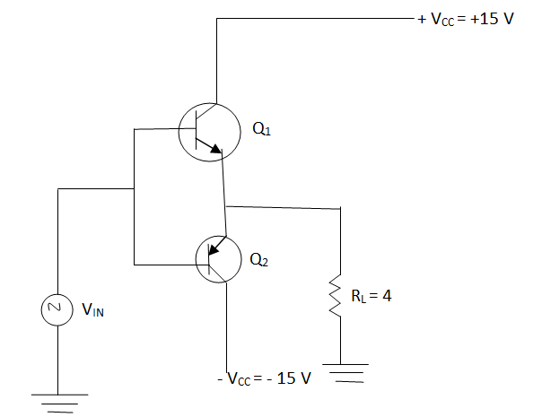
Calculate:
A2) Given: VC = 15 V, RL = 4 Ω
Use the expression derived for push pull class B.
(Pac)max = 1/2VCC2 / RL = 1/2(15)2 / 4 = 28.125 W Ans
RL = Vm / Im
Im= Vm / RL = VCC / RL = 15 / 4 = 3.75 A
Pdc = 2 / ∏VCCIm = 2 / ∏ x 1.5 x 3.75 = 35.809 W
Pd = Pdc – Pac = 35.809 – 28.125 = 7.684 W Ans.
This is the total collector dissipation under maximum power conditions.
% n = Pac / Pdc x 100 = 28.125 / 38.809 x 100 = 78.5 % Ans.
The efficiency is maximum possible for class B, due to the fact that the power developed is at its maximum.
Vm = 2 / ∏ VCC = 2 / ∏ x 15 = 9.5492 V
Im = Vm / RL = 9.5492 / 4 = 2.3873 A
Pdc = 2 / ∏ VCC Im = 2 / ∏ x 15 x 2.3873 = 22.797 W
While Pac = 1/2Vm2 / RL = 1/2(9.5492)2 / 4 = 11.398 W
(Pd)max = Pdc – Pac = 22.797 – 11.398 = 11.39 W
(Pd)max = 11.39 / 2 = 5.699 W [ Per transistor]
Alternatively, we can directly use the result,
(Pd)max = 2 / ∏2 (Pac)max per transistor
= 2 / ∏2 x 28.125 = 5.699 W per transistor Ans.
% n = Pac under (Pd)max / Pdc under (Pd)max x 100
= 11.398 / 22.797 x 100 = 50 % Ans.
This shows that when efficiency is maximum, power dissipation is not maximum and when power dissipation is maximum, efficiency is not maximum.
Q3) (A) A series fed class A amplifier uses a supply voltage of 10 V and load resistance of 20 Ω. The a.c. input voltage results in a base current of 4 mA peak. Calculate,
Assume β of the transistor as 25 and the collector bias current of 50 mA.
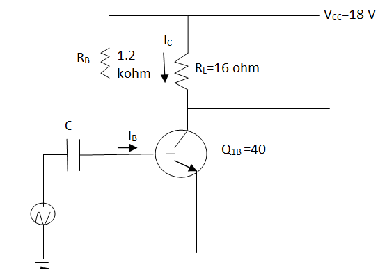
(B) Calculate the input power, output power & the efficiency of class A amplifier shown in figure. The input voltage causes a base current 5mA rms.
A3) (A) Given: VCC = 10 V, (ib)m = 4 mA, β = 25, ICQ = 50 mA, RL = 20 Ω
PDC = VCCICQ = 10 x 50 x 10-3 = 0.5 W Ans.
(ic)m = β(ib)m = 25 x 4 = 100 mA
But ic is the output current I.
Im = 100 mA
Pac = I2mRL / 2 = (100 x 10-3)2 x 20 / 2 = 0.1 W Ans.
% n = Pac / Pdc x 100 = 0.1 / 0.5 x 100 = 20 % Ans
(B) Given class A amplifier is shown in below figure

Current IBQ can be written as,
IBQ = VCC – 0.7 / RB = 18 – 0.7 / 1.2 x 103 = 14.4167 mA
Now, ICQ = βIBQ = 40 x 14.4167 = 576.67 mA
And, VCEQ = VCC – ICQ RL = 18 – 576.67 x 10-7 x 16 = 8.7733 V
So, Pdc = VCCICQ = 18 x 576.67 = 10.38 W Ans.
This is the input power.
(Ib)rms = 5 mA
(Ic)rms = β(Ib)rms = 40 x 5 = 200 mA
This is nothing but the output collector current r.m.s value Irms.
Irms = 200 mA
Output power can be written as,
Pac = I2rms RL = (200 x 10-3) x 16 = 640 mW
This is the power delivered to the load.
Hence the efficiency of the amplifier is,
% n = Pac / Pdc x 100 = 640 x 10-3 / 10.38 x 100
% n = 6.165 % Ans.
Q4) For a class B amplifier using common collector configuration, the supply voltage is 25 V while the load resistance is 16 Ω. If the input a.c. signal of 20 V peak is supplied, determine the input power, output power and the efficiency.
A4) Given: VCC = 25 V, Vm = 20 V, RL = 16 Ω
For a common collector configuration, the voltage is 1.
Vin(peak) = Vout(peak) = 20 V
Now, Vm / Im = RL
Im = Vm / RL = 20 / 16 = 1.25 A
The input power is given by,
PDC = 2 / ∏ = VCCIm = 2 / ∏ x 25 x 1.25 = 19.8943 W Ans.
The output power is given by,
Pac = Vm Im / 2 = 20 x 1.25 / 2 = 12.5 W Ans.
Thus, efficiency is given by,
% n = Pac / Pdc x 100 = 12.5 / 19.8943 x 100 = 62.832 % Ans.
Q5) What is voltage series feedback?
A5) Voltage Series Feedback: The portion of output is applied as feedback to the input voltage in series. This means that feedback circuit is located in shunt by means of the output although in series by means of the input.
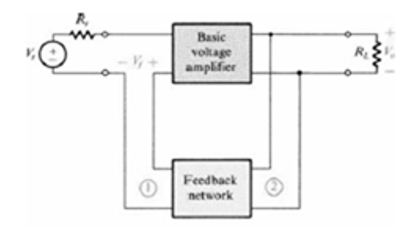
Fig. Voltage Series Feedback amplifier
Q6) What is voltage shunt feedback?
A6)
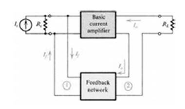
Fig. Voltage Shunt Feedback Amplifier
Q7) What is current series feedback?
A7) Current Series Feedback: In this type of feedback amplification of the signals the part of the output signal that is fed back to the input signal is related in terms of series to the feedback circuit. Due to the series connection established in the output and the input signals concerning the feedback circuit the impedance value is high at both sides.
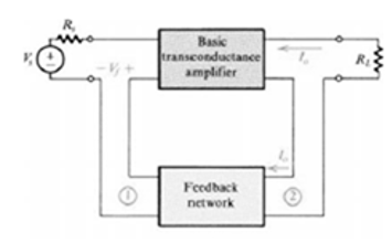
Fig. Current Series Feedback Amplifier
Q8) What is current shunt feedback?
A8) Current Shunt Feedback: The feedback circuit connected in series for the output and parallel to the input signal is known as a current shunt feedback amplifier. Due to the parallel connection with the input the value of impedance is low at this point. Whereas the output connected in terms of series makes the value of impedance high.
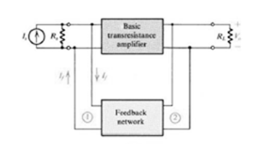
Fig. Current Shunt Feedback Amplifier
Q9) Compare all the feedback topologies?
A9)
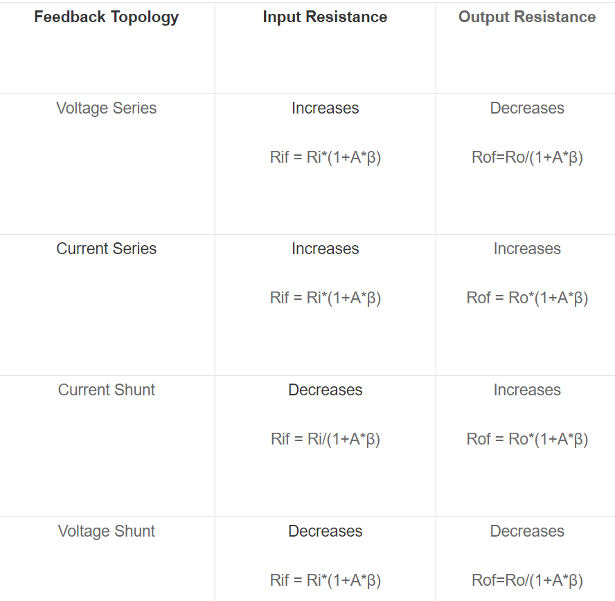
Q10) What are negative feedback amplifiers?
A10) Negative Feedback amplifier– In this type of amplifier source signal and the feedback signal are out of phase with each other. Thus, the feedback signal applied to decrease the strength of the input signal.
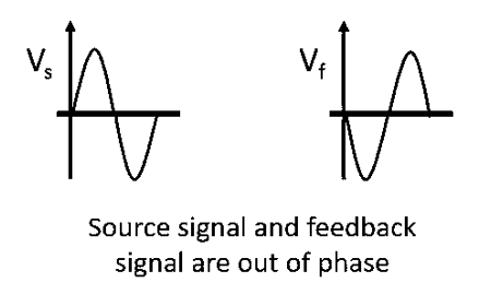
Fig. Signal out of phase
Q11) Explain principle of sinusoidal oscillator?
A11) These are known as harmonic oscillators and are LC tuned feedback or RC tuned feedback type oscillators that generate purely sinusoidal waveform which is constant in amplitude and frequency.
RC phase-shift oscillators use resistor-capacitor (RC) network as shown in Figure below to provide the phase-shift required by the feedback signal. They have excellent frequency stability and can yield a pure sine wave for a wide range of loads.
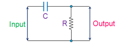
Fig. RC network
Ideally a simple RC network is expected to have an output which leads the input by 90o.The phase-difference will be less than this as the capacitor used in the circuit cannot be ideal.
Mathematically the phase angle of the RC network is expressed as
ɸ = tan -1 Xc / R
where, XC = 1/(2πfC) is the reactance of the capacitor C and R is the resistor. In oscillators, these kind of RC phase-shift networks, each offering a definite phase-shift can be cascaded to satisfy the phase-shift condition led by the Barkhausen Criterion.
Q12) Explain Wein bridge oscillator?
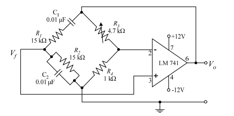
A12) Wien bridge oscillator is an audio frequency sine wave oscillator of high stability and simplicity. The feedback signal in this circuit is connected to the non-inverting input terminal so that the op-amp is working as a non-inverting amplifier.
The feedback network does not provide any phase shift. The circuit can be viewed as a Wien bridge with a series combination of R1 and C1 in one arm and parallel combination of R2 and C2 in the adjoining arm. Resistors R3 and R4 are connected in the remaining two arms.
The condition of zero phase shift around the circuit is achieved by balancing the bridge. The series and parallel combination of RC network form a lead-lag circuit.
At high frequencies, the reactance of capacitor C1 and C2 approaches zero. This causes C1 and C2 appears short. Here, capacitor C2 shorts the resistor R2. Hence, the output voltage Vo will be zero since output is taken across R2 and C2 combination. So, at high frequencies, circuit acts as a 'lag circuit'.
At low frequencies, both capacitors act as open because capacitor offers very high reactance. Again, output voltage will be zero because the input signal is dropped across the R1 and C1 combination. Here, the circuit acts like a 'lead circuit'.
But at one particular frequency between the two extremes, the output voltage reaches to the maximum value. At this frequency only, resistance value becomes equal to capacitive reactance and gives maximum output. Hence, this frequency is known as oscillating frequency (f).
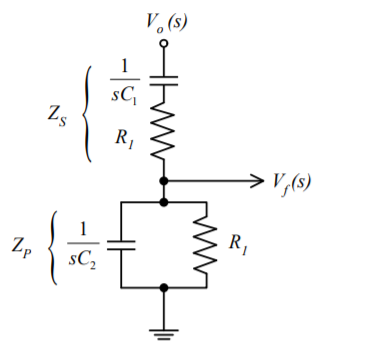
Consider the feedback circuit, on applying voltage divider rule
Vf(s) = Vo(s) x Zp(s)/ Zp(s) + Zs(s)
Zs(s) = R1 + 1/sC1 and Zp(s) = R2|| 1/sC2
Let R1=R2=R and C1=C2=C. On solving
β = Vf(s)/ Vo(s) = RsC /(RsC) 2 + 3RsC + 1 ---------------------------(1)
Since the op-amp is operated in the non-inverting configuration the voltage gain
Av = Vo(s)/ Vf(s) = 1 + R3/R4 -------------------(2)
Applying the condition for sustained oscillations, = Av β =1
RsC /(RsC) 2 + 3RsC + 1. 1 + R3/R4
S=jw
(1 + R3/R4) (jwRC/ - R2 C2 w2 + 3 jwRC + 1) =1
jw RC (1 + R3/R4) = (- R2 C2 w2 + 3 jwRC + 1)
jw [(1 + R3/R4) RC – 3RC] = 1- R2 C2 w2
To obtain the frequency of oscillation equate the real part to zero
1- R2 C2 w2 = 0
w = 1/RC
f = 1/ 2 π RC
To obtain the condition for gain at the frequency of oscillation equate the imaginary part to zero.
jw [(1 + R3/R4) RC – 3RC] = 0
jw [(1 + R3/R4) RC= jw3RC
[(1 + R3/R4) =3
R3/R4 =2
Therefore R3 = 2 R4 is the required condition.
Q13) Explain phase shift oscillator?
A13)
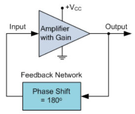
In an RC Oscillator circuit, the input is shifted 180o through the feedback circuit returning the signal out-of-phase and 180o again through an inverting amplifier stage to produces the required positive feedback.
This then gives us “180o + 180o = 360o” of phase shift which is effectively the same as 0o, thereby giving us the required positive feedback.
In other words, the total phase shift of the feedback loop should be “0” or any multiple of 360o to obtain the same effect.
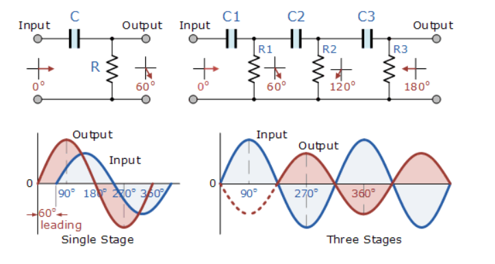
The circuit on the left shows a single resistor-capacitor network whose output voltage “leads” the input voltage by some angle less than 90o.
In a pure or ideal single-pole RC network. it would produce a maximum phase shift of exactly 90o, and because 180o of phase shift is required for oscillation, at least two single-poles networks must be used within an RC oscillator design.
However, in reality it is difficult to obtain exactly 90o of phase shift for each RC stage so we must therefore use more RC stages cascaded together to obtain the required value at the oscillation frequency.
The amount of actual phase shift in the circuit depends upon the values of the resistor (R) and the capacitor (C), at the chosen frequency of oscillations with the phase angle (φ) being given as:
Xc = 1/2π fc R=R
Z = [ R 2 + Xc 2] ½
Ø = tan -1 Xc /R
Q14) Explain crystal oscillator?
A14) Crystal Oscillator can be designed by connecting the crystal into the circuit such that it offers low impedance when operated in series-resonant mode and high impedance when operated in anti-resonant or parallel resonant mode as shown below in figure a and b respectively.
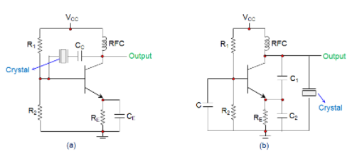
Fig. (a) Series Resonance Fig. (b) Parallel Resonance
In the circuits shown, the resistor R1 and R2 form the voltage divider network while the emitter resistor RE stabilizes the circuit. Further, CE (Figure a) acts as an AC bypass capacitor while the coupling capacitor CC (Figure a) is used to block DC signal propagation between the collector and the base terminals. Next, the capacitors C1 and C2 form the capacitive voltage divider network in the case of Figure b.
In addition, there is also a Radio Frequency Coil (RFC) in the circuits (both in Figure a and b) which offers dual advantage as it provides even the DC bias as well as frees the circuit-output from being affected by the AC signal on the power lines.
On supplying the power to the oscillator, the amplitude of the oscillations in the circuit increases until a point is reached wherein the nonlinearities in the amplifier reduce the loop gain to unity. Next, on reaching the steady-state, the crystal in the feedback loop highly influences the frequency of the operating circuit.
Further, here, the frequency will self-adjust so as to facilitate the crystal to present a reactance to the circuit such that the Barkhausen phase requirement is fulfilled.
In general, the frequency of the crystal oscillators will be fixed to be the crystal’s fundamental or characteristic frequency which will be decided by the physical size and shape of the crystal.
However, if the crystal is non-parallel or of non-uniform thickness, then it might resonate at multiple frequencies, resulting in harmonics. Further, the crystal oscillators can be tuned to either even or odd harmonic of the fundamental frequency, which are called Harmonic and Overtone Oscillators, respectively.
Q15) Compare all the Amplifiers of Class A, B, AB and C?
A15)
