Unit - 3
Pulse modulation systems
Q1) A PCM system uses a uniform quantizer followed by a 7-bit encoder. The system bit rate is 50Mbits/sec. Calculate the maximum BW of the message signal for which this system operates?
A1)
Bit rate r = 50Mbits/sec
N=7
Bit rate r=Nfs
fs=50Mbits/sec/7=7.14MHz
Maximum signal BW =fs/2 = 7.14/2= 3.57MHz
Q2) The BW of a video signal is 4.5MHz. The signal is to be transmitted using PCM with the number of quantization level Q = 1024. The sampling rate should be 20% higher than the Nyquist rate. Calculate the system bit rate?
A2)
Band width W =4.5MHz
From Nyquist rate fs= 2W= 9MHz
But fs should be 20% higher than Nyquist rate
fs = 1.2 x 9MHz = 10.8MHz
Q=2N
1024=2N
N =10
System bit rate r= Nfs = 10x10.8MHz = 108MHz
Q3) A band-limited signal m(t) of 3 kHz bandwidth is sampled at rate of 33⅓ % higher than the Nyquist rate. The maximum allowable error in the sample amplitude (i.e., the maximum quantization error) is 0.5% of the peak amplitude mp. Assume binary encoding. Find the minimum bandwidth of the channel to transmit the encoded binary signal.
A3)
The Nyquist rate is RN = 2 x 3000 Hz = 6000 Hz (samples/second), but the actual rate is 33⅓ % higher, so that is 6000 Hz + (⅓ x 6000) = 8000 Hz.
The quantization step is and the maximum quantization error is plus/minus /2. Hence, we can write
/2 =mp/L=0.5mp/100
L= 200
For binary coding, L, must be a power of two; therefore, knowing that L = 27 = 128 and 28 = 256, we must choose n = 8 to guarantee better than a 0.5% error.
Having chosen n = 8 to guarantee 0.5% error, to find the bandwidth required we note that Total number of bits per second = 8 bits 8000 Hz = 64,000 bits/second C However, we know we can transmit 2 bits/Hz of bandwidth, so it requires a bandwidth BT of
BT= C/2 =32000Hz or 32kHz
If 24 such signals are multiplexed on a single line (known as a T1 Line in the Telephone system, then CT1 = 24 x 64 kb/s = 1.536 Mb/s, and the bandwidth is 768 KHz.
Q4) We are given a signal m(t) = 2cos (2250 t) as the signal input. Find the SNR with 8-bit PCM.
A4)
For 8-bit encoding, L = 2n where n = 8, therefore, the number of levels = 256.
The amplitude Am of the sinusoidal waveform means that mp = 2 volts.
The total signal swing possible (- mp to + mp) will be 2mp = 4 volts, therefore, the average signal power is Pave = [(Am )2 /2] = [22/2] = 2 watts.
The interval = [2mp /L] = 4 volts/256 levels = 1.625 10-2 volt
Using for the quantization noise Nq = [()2 /12], and taking Pave = 2 W, the SNR is given by


Q5) We are given a signal m(t) = 2cos (2250 t) as the signal input. If the minimum SNR is to be at least 36 dB, how many bits n are needed to encode the signal (i.e., find n)? Use signal power as mentioned in Q4.
A5)
Note that 36 dB is numerically equivalent to 3,981 [about 4,000].
Remembering that the interval is = [2mp /L] and
2mp = 4 volts.

Therefore, we can determine the number of levels L, and then n.

The lowest integer number of bits n that will give at least 31.5 levels is n = 5 because 25 = 32 levels.
So, the answer is 5 bits.
Q6) The number of bits in a binary PCM system is increased from n to n+1. As a result, the signal quantization noise ratio will improve by a factor
A6)
(a) (n+ 1)/n
(b) 2(n+1) /n
(c) 4
(d)Which is independent of n.
A6)

For 


Q7) The bandwidth required for the transmission of a PCM signal increases by a factor of _____when the number of quantization levels is increased from 4 to 64.
A7)
(a) 2 Times (b) 3 Times (c) 4 Times (d)Which is independent of quantization levels
A7)


Q8) A sinusoidal signal with peak-to-peak amplitude of 1.536 V is quantized into 128 levels using a midtread uniform quantizer. The quantization noise power is
A8)
(a) 0.768 V (b)48 × 10-6 v2 (c) 12 × 10-6 v2 (d)3.072 V
A8)


Q9) In a PCM system, the signal m(t) = {sin (100πt) + cos(100πt)} V is sampled at the Nyquist rate. The samples are processed by a uniform quantizer with step size 0.75 V. The minimum data rate of the PCM system in bits per second is?
A9)
Nyquist rate =2x50=100 samples/s
Step size = m(t)max - m(t)min/L
Number of levels L = √2-(-√2)/0.75 = 4
Number of bits required to encode 4 levels = 2bits/level
Data rate = 2x100=200 bits/s
Q10) A television signal with a bandwidth of 4.2 Mz is transmitted using binary PCM. The number of quantization levels are 512. Calculate (a) code word length (b) Transmission bandwidth (c) Final bit rate (d) Output signal to quantization noise ratio
A10)
Signal Bandwidth =4.2 MHz, N=512
(a) n= codeword length 

(b) Bandwidth 
(c) Final bit rate 

Bit rate 

Q11) Twelve different message signals each of bandwidth 20kHz are to be multiplexed and transmitted. Determine the minimum bandwidth required for PAM/TDM system?
A11)
No. Of channels N =12
Bandwidth of each channel fm = 20kHz
Minimum bandwidth required to avoid crosstalk is = Nfm = 20 x 12 = 240kHz
Q12) Compare various pulse modulation schemes?
A12)
SR. NO. | PARAMETER | PAM | PWM | PPM |
1 | Type of Carrier | Train of Pulses | Train of Pulses | Train of Pulses |
2 | Variable Characteristic of the Pulsed Carrier | Amplitude | Width | Position |
3 | Bandwidth Requirement | Low | High | High |
4 | Noise Immunity | Low | High | High |
5 | Information Contained in | Amplitude Variations | Width Variations | Position Variations |
6 | Transmitted Power | Varies with amplitude of pulses | Varies with variation in width | Remains Constant |
7 | Need to transmit synchronizing pulses | Not needed | Not needed | Necessary |
8 | Complexity of generation and detection | Complex | Easy | Complex |
9 | Similarity with other Modulation Systems | Similar to AM | Similar to FM | Similar to PM |
10 | Output waveforms | Refer Figure down | Refer Figure down | Refer Figure down |
Q13) What are eye patterns explain?
A13)
An eye diagram or eye pattern is simply a graphical display of a serial data signal with respect to time that shows a pattern that resembles an eye.
The signal at the receiving end of the serial link is connected to an oscilloscope and the sweep rate is set so that one- or two-bit time periods (unit intervals or UI) are displayed. This causes bit periods to overlap and the eye pattern to form around the upper and lower signal levels and the rise and fall times. The eye pattern readily shows the rise and fall time lengthening and rounding as well as the horizontal jitter variation.
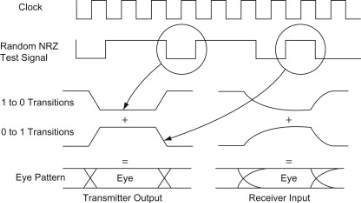
Fig. 1: Eye diagram
Q14) What is inter symbol interference and also mention its cause?
A14)
This is a form of distortion of a signal, in which one or more symbols interfere with subsequent signals, causing noise or delivering a poor output.
Causes of ISI
The main causes of ISI are −
- Multi-path Propagation
- Non-linear frequency in channels
The ISI is unwanted and should be completely eliminated to get a clean output. The causes of ISI should also be resolved in order to lessen its effect.
To view ISI in a mathematical form present in the receiver output, we can consider the receiver output.
The receiving filter output y(t)y(t) is sampled at time ti=iTb (with i taking on integer values), yielding –
y(ti)= μ∑akp(iTb−kTb)
= μai+μ∑akp(iTb−kTb)
In the above equation, the first term μai is produced by the ith transmitted bit.
The second term represents the residual effect of all other transmitted bits on the decoding of the ith bit. This residual effect is called as Inter Symbol Interference.
In the absence of ISI, the output will be −
y(ti)=μai
This equation shows that the ith bit transmitted is correctly reproduced. However, the presence of ISI introduces bit errors and distortions in the output.
While designing the transmitter or a receiver, it is important that you minimize the effects of ISI, so as to receive the output with the least possible error rate.
Q15) What is cross talk in TDM of PCM?
A15)
There should always be synchronisation in transmitter and receiver. Usually, markers are inserted to indicate the separation between the frames. Synchronisation is obtained due to these marker pulses but the number of channels to be multiplexed is reduced by one. They become N-1.
Crosstalk
In TDM transmission the signal is converted to smooth modulating waveform when passed through the baseband filter. The baseband value passes through the values of all the individual samples.
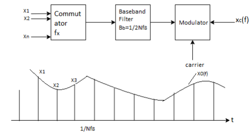
Fig 2 TDM transmission with baseband filtering and its waveform
Due to this baseband filter crosstalk arises in between two samples. This interference can be reduced by increasing the distance between individual signal samples. The minimum distance required to avoid crosstalk between two samples is called as guard time.
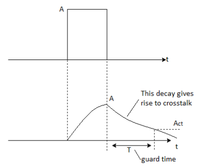
Fig 3 Applied rectangular pulse and its response
From above figure we see that even after the pulse is removed the response decays from its value A and then takes longer period. The guard time Tg represents minimum pulse spacing. After guard time end the pulse tail is less than Act.
Act = A
B= Bandwidth of signal
Q16) Explain PTM systems?
A16)
There are two types of PTM systems. They are Pulse width modulation (PWM) and Pulse Position Modulation (PPM).
Pulse Width Modulation
In this type of modulation, the amplitude is maintained constant but the width of each pulse is varied in accordance with instantaneous value of the analog signal. In PWM information is contained in width variation. This is similar to FM. In pulse width modulation (PWM), the width of each pulse is made directly proportional to the amplitude of the information signal.
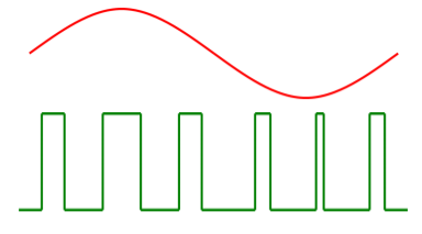
Fig 4 PWM waveform
PPM
In this type of modulation, the sampled waveform has fixed amplitude and width whereas the position of each pulse is varied as per instantaneous value of the analog signal. PPM signal is further modification of a PWM signal.
PPM and PWM modulator

Fig 4 PTM Modulator
- The PPM signal can be generated from PWM signal.
- The PWM pulses obtained at the comparator output are applied to a mono stable multi vibrator which is negative edge triggered.
- Hence for each trailing edge of PWM signal, the monostable output goes high. It remains high for a fixed time decided by its RC components.
- Thus, as the trailing edges of the PWM signal keeps shifting in proportion with the modulating signal, the PPM pulses also keep shifting.
- Therefore, all the PPM pulses have the same amplitude and width. The information is conveyed via changing position of pulses.

Fig 5 PWM and PPM Modulation waveforms.
PWM Demodulator
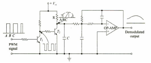
Fig 6 PWM Demodulator
- Transistor T1 works as an inverter.
- During time interval A-B when the PWM signal is high the input to transistor T2 is low.
- Therefore, during this time interval T2 is cut-off and capacitor C is charged through an R-C combination.
- During time interval B-C when PWM signal is low, the input to transistor T2 is high, and it gets saturated.
- The capacitor C discharges rapidly through T2.
- The collector voltage of T2 during BC is low.
- Thus, the waveform at the collector of T2is similar to saw-tooth waveform whose envelope is the modulating signal.
- Passing it through 2nd order op-amp Low Pass Filter, gives demodulated signal.
PPM Demodulator
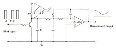
Fig 7 PPM Demodulator
- The gaps between the pulses of a PPM signal contain the information regarding the modulating signal.
- During gap A-B between the pulses the transistor is cut-off and the capacitor C gets charged through R-C combination.
- During the pulse duration B-C the capacitor discharges through transistor and the collector voltage becomes low.
- Thus, waveform across collector is saw-tooth waveform whose envelope is the modulating signal.
- Passing it through 2nd order op-amp Low Pass Filter, gives demodulated signal.
Q17) With help of circuit diagram explain the PAM system?
A17)
In PAM, amplitude of pulses is varied in accordance with instantaneous value of modulating signal.
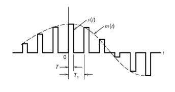
Fig 8 PAM waveform
PAM Generation:
The carrier which is in the form of narrow pulses has frequency fc. The uniform sampling takes place in multiplier to generate PAM signal. Samples are placed Ts sec away from each other.
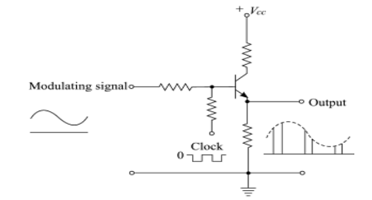
Fig 9 PAM Modulator
- The circuit is simple emitter follower.
- In the absence of the clock signal, the output follows input.
- The modulating signal is applied as the input signal.
- Another input to the base of the transistor is the clock signal.
- The frequency of the clock signal is made equal to the desired carrier pulse train frequency.
- The amplitude of the clock signal is chosen the high level is at ground level(0v)
- Low level at some negative voltage sufficient to bring the transistor in cut-off region.
- When clock is high, circuit operates as emitter follower and the output follows in the input modulating signal.
- When clock signal is low, transistor is cut-off and output is zero.
- Thus, the output is the desired PAM signal.
PAM Demodulator:
The PAM demodulator circuit which is just an envelope detector followed by a second order op-amp low pass filter (to have good filtering characteristics) is as shown below

Fig 10 PAM Demodulator
Q18) What are the basic elements of PCM?
A18)
Basic Elements of PCM
The transmitter section comprises of Sampling, Quantizing and Encoding. The low pass filter prior to sampling prevents aliasing of the message signal.
The basic operations in the receiver section are regeneration of impaired signals, decoding, and reconstruction of the quantized pulse train.
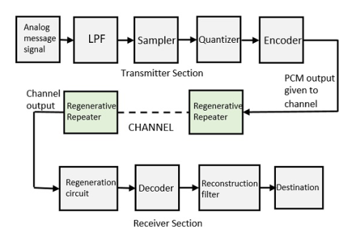
Fig.11: PCM
Low Pass Filter
This filter eliminates the high frequency components present in the input analog signal to avoid aliasing of the message signal.
Sampler
It helps to collect the sample data at instantaneous values of message signal, so as to reconstruct the original signal. The sampling rate must be in accordance with the sampling theorem.
Quantizer
It reduces excessive bits and confines the data. It reduces the redundant bits and compresses the value of the sampled output.
Encoder
The digitization of analog signal is done by the encoder. It designates each quantized level by a binary code. Encoding minimizes the bandwidth used.
Regenerative Repeater
It increases the signal strength. The output of the channel also has one regenerative repeater circuit, to compensate the signal loss and reconstruct the signal, and also to increase its strength.
Decoder
The decoder circuit decodes the pulse coded waveform to reproduce the original signal. This circuit acts as the demodulator.
Reconstruction Filter
After the digital-to-analog conversion is done by the regenerative circuit and the decoder, a low-pass filter is employed, called as the reconstruction filter to get back the original signal.
Hence, the Pulse Code Modulator circuit digitizes the given analog signal, codes it and samples it, and then transmits it in an analog form. This whole process is repeated in a reverse pattern to obtain the original signal.
Q19) What is companding. Explain A-law and µ-law Companding Technique
A19)
There are two types of Quantization - Uniform Quantization and Non-uniform Quantization.
The type of quantization in which the quantization levels are uniformly spaced is termed as a Uniform Quantization. The type of quantization in which the quantization levels are unequal and mostly the relation between them is logarithmic, is termed as a Non-uniform Quantization.
Companding
It is a combination of Compressing and Expanding, which means that it does both. This is a non-linear technique used in PCM which compresses the data at the transmitter and expands the same data at the receiver. The effects of noise and crosstalk are reduced by using this technique.
There are two types of Companding techniques. They are −
A-law Companding Technique
- Uniform quantization is achieved at A = 1, where the characteristic curve is linear and no compression is done.
- A-law has mid-rise at the origin. Hence, it contains a non-zero value.
- A-law companding is used for PCM telephone systems.
µ-law Companding Technique
- Uniform quantization is achieved at µ = 0, where the characteristic curve is linear and no compression is done.
- µ-law has mid-tread at the origin. Hence, it contains a zero value.
- µ-law companding is used for speech and music signals.
µ-law is used in North America and Japan.
Q20) Derive SNR for PCM systems?
A20)
Signal to noise ratio in PCM:
SNR= (signal power)/ (noise power)
Signal power=p Quantization error=ἐ=xq(nT)-x(nT) =(xmax-xmin)/2n
Where, n is code word length.
|e| =
Quantization noise power=E[e2]
 (limits from - to )
 (limits from - to )


If the signal is defined from –xmax to +xmax
Then Δ =(2xmax)/2n
(S/N) PCM=(12p)/(2xmax/2n)2
=(12p*22n)/(4xmax2)
=(3p*22n)/xmax2
For normalized signal xmax=1
Then SNR for normalized signal is slightly less than or equal to 3.1*22n i.e.
(S/N) PCM for normalized signal≤3.1*22n
(S/N) PCM in dB=10log10(3*22n) =4.8+6n
For increasing one bit then (S/N) PCB will increase to 6dB.