Unit - 5
Operational Amplifier
Q1) A 200mV peak to peak sine waveform voltage is applied to Op-amp inverting amplifier with Rf/R1 = 10.
A1) Peak to peak input voltage
2Vm = 200 mV
Vm = 100 mV
Vi= Vm sin wt = 100 sin wt mV
Vo = -Rf/R1 x vi = -10 x 100 sinwt mV
= -1000 sin wt mV
Q2) Design a non-inverting amplifier using Op-amp with a closed loop voltage gain of 10.
A2) Af = 1 + Rf/R1 =10
Rf/R1 = 9
Rf = 9 R1
If R1 = 1K
Rf = 9K Ω
Q3) In an op-amp inverting amplifier R1 = 1K Ω and Rf = 100KΩ. The DC supply voltage of the op-amp is ± 15V. Calculate the output voltage if input voltage is 1V.
A3) R1 = 1KΩ Rf = 100KΩ
V+ = 15V and V-=-15V. vi = 1V
Af = -Rf/R1 = -100K/1K = -100
Af = vo/vi
Vo = Af vi
= -100 x 1V = -100V
The output voltage cannot exceed the DC power supply voltage. Since vo is negative and large it is limited to V-
Vo ≈ V- = -15V
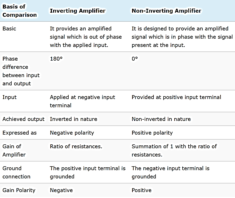
Q4) Compare inverting, non-inverting and differential amplifier?
A4)
Q5) Explain voltage series amplifier?
A5) In the voltage series feedback circuit, a fraction of the output voltage is applied in series with the input voltage through the feedback circuit. This is also known as shunt-driven series-fed feedback, i.e., a parallel-series circuit.
The following figure shows the block diagram of voltage series feedback, by which it is evident that the feedback circuit is placed in shunt with the output but in series with the input.
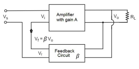
Fig 1 Voltage Series Feedback
As the feedback circuit is connected in shunt with the output, the output impedance is decreased and due to the series connection with the input, the input impedance is increased.
Q6) Derive Av, Ri, Ro for voltage series feedback amplifier?
A6) Voltage series:
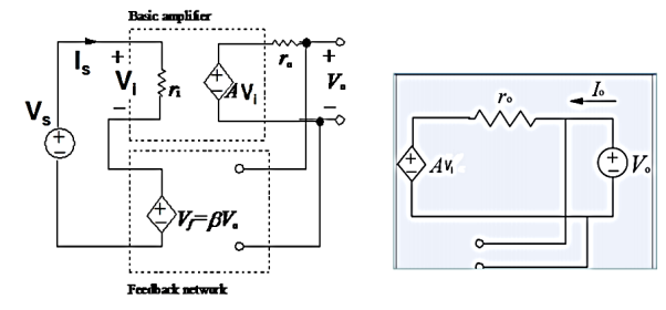
Fig 2 Voltage Series Feedback
Voltage Gain:
Vo = A.Vi
Vf = β Vo
A (Vs – βVo) = Vo
AVs = (1+βA) Vo
Af = Vo/Vs = A/1+βA
Input impedance
Zin = Vs/Is = Vi+βAVi/Is
Zin = Vi (1+β A) /Is = ri(1+βA)
Output Impedance
Zout IVS=0 = Vo/Io
Io = Vo – A. Vi / ro
Vi + β. Vo = Vs
Vi = - β Vo
Io = Vo + AβVo/ro
Zout = Vo/Io = ro / 1+Aβ
Q7) Derive Av, Ri, Ro for voltage shunt feedback amplifier?
A7) Voltage shunt feedback amplifier:

Fig 3 Voltage shunt feedback network
Voltage gain:
Vo =A.Ii = A(Is – If)
If = β Vo
A (Is – β Vo) = Vo
A Is = (1+βA) Vo
Af = Vo/Is = A/ 1+βA
Input Impedance
Zin = Vi/Is = Vi/ Ii + If
= Ii. ri / Ii + β A Ii
Zin = ri / (1+βA)
Output Impedance
Zout IVS =0 = Vo/Io
From input port
Ii = -If = - β Vo
From output port
Io = Vo – A Ii/ro = Vo + βAVo/ro
Zo = Vo /Io = ro/ (1+βA)
Q8) Explain open loop frequency response of op-amp?
A8) “Open Loop Gain” which is defined as the amplifiers output amplification without any external feedback signals connected to it and for a typical operational amplifier is about 100dB at DC (zero Hz). This output gain decreases linearly with frequency down to “Unity Gain” or 1, at about 1MHz and this is shown in the following open loop gain response curve.
Open-loop Frequency Response Curve
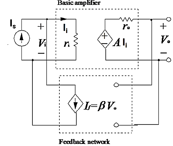
Fig 4 Frequency Response Curve
From this frequency response curve, we can see that the product of the gain against frequency is constant at any point along the curve. Also, that the unity gain (0dB) frequency also determines the gain of the amplifier at any point along the curve. This constant is generally known as the Gain Bandwidth Product or GBP. Therefore:
GBP = Gain x Bandwidth = A x BW
For example, from the graph above the gain of the amplifier at 100kHz is given as 20dB or 10, then the gain bandwidth product is calculated as:
GBP = A x BW = 10 x 100,000Hz = 1,000,000.
Similarly, the operational amplifiers gain at 1kHz = 60dB or 1000, therefore the GBP is given as:
GBP = A x BW = 1,000 x 1,000Hz = 1,000,000.
The Voltage Gain (AV) of the operational amplifier can be found using the following formula:
Av = Vout/ Vin
and in Decibels or (dB) is given as:
20 log (A) or 20 log (Vout/ Vin ) in dB
An Op- Amp Bandwidth
The operational amplifiers bandwidth is the frequency range over which the voltage gain of the amplifier is above 70.7% or -3dB (where 0dB is the maximum) of its maximum output value.

Fig 5 Frequency Response
Q9) Explain slew rate and also derive its expression?
A9) The slew rate is a parameter that describes the operating speed of an op-amp. It represents the rate that can change per unit time stipulated by the output voltage.
For example, 1V/us indicates that the voltage can change by 1V in 1μs. Ideal op-amps make it possible to faithfully output an output signal for any input signal. However, in reality slew rate limits do exist.
When supplying a rectangular pulse at the input with a steep rise and fall, this indicates the possible degree of change in the output voltage per unit time.

Fig 6 Slew Rate calculation
The rise and fall slew rates are calculated by the following equations:
SRr = ∆ V / ∆ Tr
SRf = ∆ V / ∆ Tf

Fig 7 Sinusoidal waveform
Calculate the slew rate
The output is given by
y=Asinωt
The slew rate is the slope of the tangent of the sine wave, differentiating the above equation.
dy / = Aω cosωt ωt=0
Dt
The slew rate is
SR=Aω ω=2πf

Fig 8 Sinusoidal Waveform
Since the amplitude of the sine wave becomes Vpp=2A (peak-to-peak), the equation can be modified as follows.

This frequency(f) is referred to as the full power bandwidth. These are conditions where the amplification factor in the op-amp has not been set, in other words the relationship of the frequency and amplitude (within the output voltage range) that can be output by the op-amp in a voltage follower circuit.
Q10) Define thermal drift?
A10) It is defined as the change in output offset voltage due to change in temperature. Its unit is  V/0C.
V/0C.
Thermal Drift = 
The thermal drift in input offset current = 
The thermal drift in input bias current = 
Q11) Define CMRR for op-amp?
A11) It is the ratio of differential voltage gain Ad to the common mode voltage gain Acm.
CMRR = 
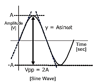
Fig 9 Common Mode Configuration
The common mode voltage gain from above figure can be
 =
= 
Where:
Vocm = output common mode voltage
Vcm = input common mode voltage
Acm = common mode voltage gain
In normal cases the value of Ad is large and Acm is very small making the value of CMRR very high.
Q12) Define SVRR for op-amp?
A12) The Power Supply Rejection Ratio (PSRR) is also known as Supply Voltage Rejection Ratio (SVRR). It is defined as the change in op-amps input offset voltage due to variations in the supply voltage.
PSRR = 
 = Change in input offset voltage
 = Change in supply voltage
Q13) Draw the block diagram for op-amp and explain its working?
A13)

Fig 10 Block Diagram of Operational Amplifier (Op-Amp)
Q14) Mention in detail all the op-amp specifications?
A14) An Operational Amplifier is basically a three-terminal device which consists of two high impedance inputs. One of the inputs is called the Inverting Input, marked with a negative or “minus” sign, (–). The other input is called the Non-inverting Input, marked with a positive or “plus” sign (+).
A third terminal represents the operational amplifiers output port which can both sink and source either a voltage or a current.
In a linear operational amplifier, the output signal is the amplification factor, known as the amplifiers gain (A) multiplied by the value of the input signal and depending on the nature of these input and output signals, there can be four different classifications of operational amplifier gain.
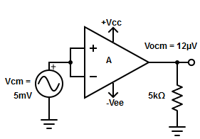
Fig 11 Operational Amplifier
Practical op-amps have zero offset voltage. The bandwidth of the practical op-amp is very small. This output can be raised to the required value by adjusting the negative feedback. The equivalent circuit is shown below.

Fig 12 Practical Op-Amp
The input impedance Zi ranges to mega ohms. The output impedance Z0 is in the order of ohms and the practical op-amps have high value of open loop voltage gain AV. The value of CMRR and Slew rate should be as high as possible.
Q15) Draw the transfer characteristics of op-amp?
A15)
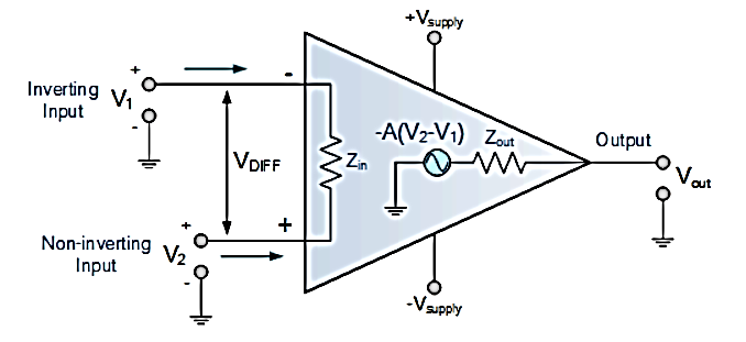
Fig 13 Transfer characteristics of ideal op-amp
Open Loop Gain (Avo)
The main function of an operational amplifier is to amplify the input signal and the more open loop gain it has the better. Open-loop gain is the gain of the op-amp without positive or negative feedback and for such an amplifier the gain will be infinite
Input impedance (ZIN)
Input impedance is the ratio of input voltage to input current and is assumed to be infinite to prevent any current flowing from the source supply into the amplifiers input circuitry (IIN = 0). Real op-amps have input leakage currents from a few pico-amps to a few milli-amps.
Output impedance (ZOUT)
The output impedance of the ideal operational amplifier is assumed to be zero acting as a perfect internal voltage source with no internal resistance so that it can supply as much current as necessary to the load. This internal resistance is effectively in series with the load thereby reducing the output voltage available to the load. Real op-amps have output impedances in the 100-20kΩ range.
Bandwidth (BW)
An ideal operational amplifier has an infinite frequency response and can amplify any frequency signal from DC to the highest AC frequencies, so it is therefore assumed to have an infinite bandwidth.
With real op-amps, the bandwidth is limited by the Gain-Bandwidth product (GB), which is equal to the frequency where the amplifiers gain becomes unity.
Offset Voltage (VIO)
The amplifiers output will be zero when the voltage difference between the inverting and the non-inverting inputs is zero, the same or when both inputs are grounded. Real op-amps have some amount of output offset voltage.
Q16) What is off set voltage of op-amp?
A16) With an input offset voltage and a differential input circuit, ideal op-amps and comparators will have an offset voltage of 0V, including error voltage.
When inputting a common-mode (same) voltage to the input pins of an op-amp or comparator, with an ideal op-amp no output voltage will be output
In case where an input offset voltage exists, a voltage will be output based on the input offset voltage. This input offset voltage, which is the differential voltage required to make the output voltage 0V, becomes the input conversion value.
The Offset voltage is normally expressed in units of mV or µV. Values closer to 0 are more ideal.
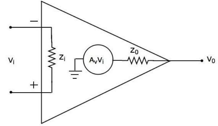
Fig 14 Op-Amp Parameters
The output offset voltage is the voltage at the output when the differential input voltage is zero.
Q17) Explain the input and output offset currents?
A17) Bias current compensation will work if both bias currents IB+ and IB- are equal. Since the input transistor cannot be made identical. There will always be some small
difference between IB+ and IB-. This difference is called the offset current
|Ios| = IB+-IB------------------------- (7)
Offset current Ios for BJT op-amp is 200nA and for FET op-amp is 10pA. Even with bias current compensation, offset current will produce an output voltage when Vi = 0.
V1 = IB + R comp
And I1 = V1 R1
KCL at node a gives
I2 = (  – I1) =
  - (Ib + Rcomp/R1)
Again V0 = I2 Rf – V1
Vo = I2 Rf - IB+ Rcomp
Vo = 1M Ω X 200nA
Vo = 200mV with Vi = 0
Q18) For inverting op-amp explain the input bias current?
A18) The op-amp‘s input is differential amplifier, which may be made of BJT or FET.
In an ideal op-amp, we assumed that no current is drawn from the input terminals the base currents entering into the inverting and non-inverting terminals (IB- & IB+ respectively).
Even though both the transistors are identical, IB- and IB+ are not exactly equal due to internal imbalance between the two inputs. Manufacturers specify the input bias current IB

Fig 15 Input Bias Current Configuration
If input voltage Vi = 0V. The output Voltage Vo should also be (Vo = 0) but for IB = 500nA We find that the output voltage is offset by Op-amp with a 1M feedback resistor
Vo = 500nA X 1M = 500mV
The output is driven to 500mV with zero input, because of the bias currents.
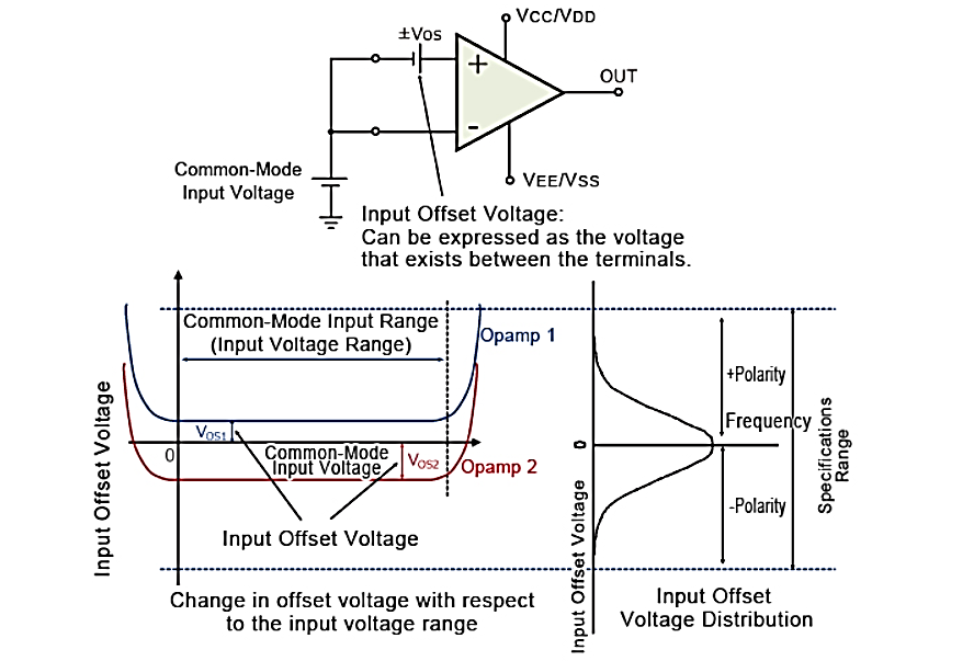
Fig 16 Input Bias Current Compensation
Current IB+ flowing through the compensating resistor Rcomp, then by KVL we get,
- V1+0+V2-Vo = 0 (or)
Vo = V2 – V1 --------- (1)
By selecting proper value of Rcomp, V2 can be cancelled with V1 and the Vo = 0. The value of Rcomp is derived as
V1 = IB+Rcomp (or)
IB+ = V1/Rcomp ------------------------ (2)
The node ‘a’ is at voltage (-V1). Because the voltage at the non-inverting input terminal is (-V1). So, with Vi = 0 we get,
I1 = V1/R1 ------------------------ (3)
I2 = V2/Rf ------------------------ (4)
For compensation, Vo should equal to zero (Vo = 0, Vi = 0). i.e., from equation (3) V2 = V1. So that,
I2 = V1/Rf ——> (5)
KCL at node ‘a’ gives,
IB- = I2 + I1 = (V1/Rf) +(V1/R1) = V1(R1+Rf)/R1Rf ------------------------ (5)
Assume IB- = IB+ and using equation (2) & (5) we get
V1 (R1+Rf)/R1Rf = V1/Rcomp
Rcomp = R1 || Rf ------------------------ (6)
i.e., to compensate for bias current, the compensating resistor, Rcomp should be equal to the parallel combination of resistor R1 and Rf.