Unit - 2
Combinational Digital Circuits
Q1) What is a Multiplexer? Explain 2:1 Mux in detail.
A1)
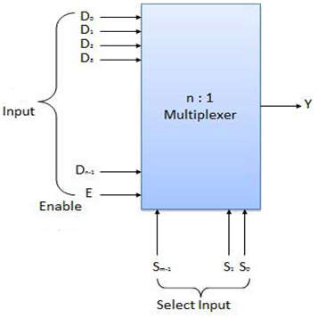
Block diagram of multiplexer
Multiplexers come in multiple variations
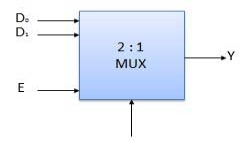
Block Diagram of 2:1 MUX
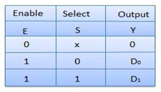
Truth Table of 2:1 MUX
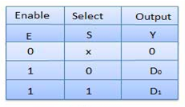
Where x is don’t care.
Q2) Draw and explain Full adder.
A2)
Block diagram
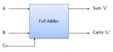
Full adder
Truth Table
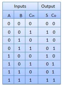
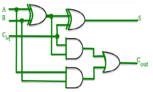
Circuit Diagram
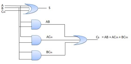
Full adder
Q3) Draw and explain Full Subtractor.
A3)
Truth Table
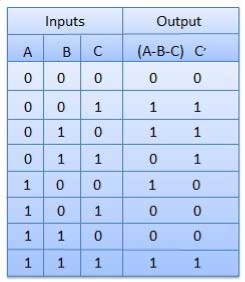
Circuit Diagram
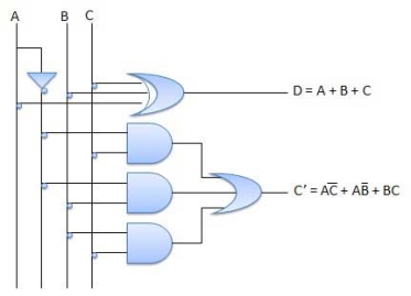
Full subtractor
Q4) Do BCD addition of 0101 with 0110.
A4)
Check your self.

Q5) Explain look ahead carry adder with circuit diagram.
A5)

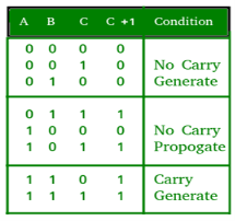
Look ahead Carry adder
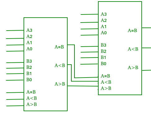
Q6) Explain digital comparator with its applications.
A6)
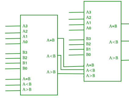
Digital comparator
Applications of Comparators –
Q7) Explain even parity generator with example.
A7) A 3-bit message is transmitted with an even parity bit. Hence assuming, the three inputs W, X and Y that are applied to the circuits and output bit is the parity bit P. The total number of 1s must be even, to generate the even parity bit P.
3- bit message | Even Parity | ||
W | X | Y | P |
0 | 0 | 0 | 0 |
0 | 0 | 1 | 1 |
0 | 1 | 0 | 1 |
0 | 1 | 1 | 0 |
1 | 0 | 0 | 1 |
1 | 0 | 1 | 0 |
1 | 1 | 0 | 0 |
1 | 1 | 1 | 1 |
The K-map simplification for 3-bit message even parity generator is
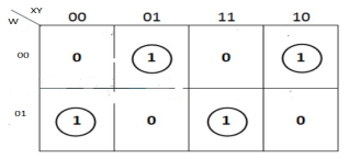
From the above K-Map, the expression is:
P=W′X′Y+W′XY′+WX′Y′+WXY
P=W′(X′Y+XY′) +W(X′Y′+XY)
P=W′(X⊕Y) +W(X⊕Y) ′=W⊕X⊕Y

Q8) Explain even parity checker with example.
A8) Assume a 3-bit binary input, W, X and Y is transmitted along with an even parity bit, P. So, the resultant data contains 4 bits, that is received as the input of even parity checker.
It generates an even parity bit, E. This bit is zero, if the received data contains an even number of ones, which indicates that there is no error in the received data and vice versa.
The Truth table of an even parity checker is:
4-bit Received Data WXYP | Even Parity Check Bit E |
0000 | 0 |
0001 | 1 |
0010 | 1 |
0011 | 0 |
0100 | 1 |
0101 | 0 |
0110 | 0 |
0111 | 1 |
1000 | 1 |
1001 | 0 |
1010 | 0 |
1011 | 1 |
1100 | 0 |
1101 | 1 |
1110 | 1 |
1111 | 0 |
The Boolean function of even parity check bit as
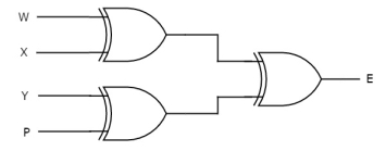
E = W xor X xor Y xor P
The following figure shows the circuit diagram of even parity checker.
Q9) Convert Gray code To Binary Code.
A9)

Then the K-maps:

And B3 = G3
The realization of Gray-to-Binary converter is
Q10) Implement 3:8 Decoder.
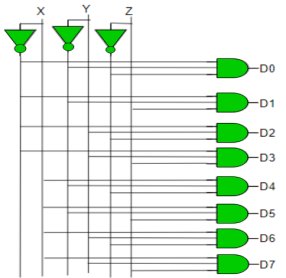
A10) D0 is high when X = 0, Y = 0 and Z = 0. Hence,
D0 = X’ Y’ Z’
Similarly,
D1 = X’ Y’ Z
D2 = X’ Y Z’
D3 = X’ Y Z
D4 = X Y’ Z’
D5 = X Y’ Z
D6 = X Y Z’
D7 = X Y Z
Hence,
Decoder