Unit - 2
Thyristor rectifiers
Q1) Explain single phase half wave rectifier?
A1) A single- phase half -wave controlled rectifier circuit consists of SCR / thyristor, an AC voltage source and load. The load may be purely resistive, Inductive or a combination of resistance and inductance.
For simplicity, we will consider a resistive load.
A simple circuit diagram of Single- Phase Half Wave Controlled Rectifier is shown in figure below.
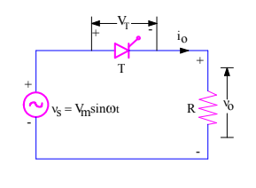
Half wave rectifier
v0 = Load output voltage
i0 = Load current
VT = Voltage across the thyristor T
The key points in controlled rectifier are:
Let us assume that thyristor T is fired at a firing angle of α. This means when wt = α, gate signal will be applied and SCR will start conducting.
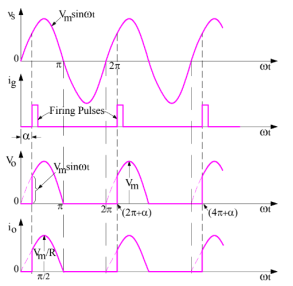
Figure. Output Waveforms
Thyristor T is forward biased for the positive half cycle of supply voltage. The load output voltage is zero till SCR is fired. Once SCR is fired at an angle of α, SCR starts conducting. But as soon as the supply voltage becomes zero at ωt = π, the load current will become zero and after ωt = π, SCR is rever
sed biased. Thus, thyristor T will turn off at ωt = π and will remain in OFF condition till it is fired again at ωt = (2π+α).
Therefore, the load output voltage and current for one complete cycle of input supply voltage may be written as
v0 = VmSinωt for α≤ωt≤ π
i0 = VmSinωt / R for α≤ωt≤ π
Q2) Explain the calculation of output voltage?
A2) Calculation of Average Load Output Voltage:
As we know that, average value of any function f(x) cab be calculated using the formula
Average value = (1/T)  dx
dx
Let us now calculate the average value of output voltage for Single Phase Half Wave Controlled Rectifier.
Average value of load output voltage
= (1/2π)  sin wt d(wt)
= (1/2π)  sin wt d(wt) +
  sin wt d(wt) +
  sin wt d(wt)
Since the value of load output voltage is zero from 0≤wt ≤ α and π≤wt  2π therefore
= (1/2π)  sin wt d(wt)
= (Vm/2π)  sin wt d(wt)
= (Vm/2π) [ 1 + cos α]
For single phase half -wave controlled rectifier
Average value of load output voltage
= (Vm/2 ) [ 1+cos α]
From the expression of average output voltage, it can be seen that, by changing firing angle α, we can change the average output voltage. The average output voltage is maximum when firing angle is zero and it is minimum when firing angle α = π. This is the reason, it is called phase-controlled rectifier.
Average load current for Single Phase Half Wave Controlled Rectifier can easily be calculated by dividing the average load output voltage by load resistance R.
Q3) Explain Single phase full bridge thyristor rectifier with R load?
A3) The figure shows a full wave-controlled bridge rectifier circuit with a resistive load. In this circuit, diagonally opposite pairs of SCRs turn on and off together.
During the positive half-cycle of the input voltage, SCRl is forward-biased. If we apply the gate signal at a SCRl turns on. The output Voltage (Vo) follows the input voltage. The load current (io = vo/R|) has the same waveform as the load voltage. At π, when the current through SCR1 becomes zero, it turns off naturally.
During the negative half-cycle; SCR2 is forward biased. SCR2 is fired at (π+α). The output voltage again follows the input voltage. The current through SCR2 becomes zero at 2 π; and it turns off. SCR2 is fired again at (2π+α) and SCR2 at (3π+α), and the cycle repeats.
Figure shows the resulting voltage and current waveforms.
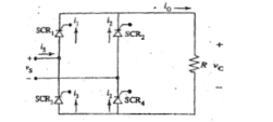
Figure (a) . Full wave controlled bridge rectifier with R load
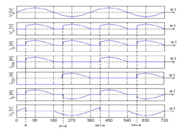
Output Waveform
The average value of the output DC volatge is given by
Vo(avg) = 1/2π 2  2 V sin(wt) dwt = 1/2π 2
  Vm sin(wt) dwt
Vo(avg) = Vm/π (1+cosα)
Io(avg) = Vo(avg)/R = Vm/πR(1+cosα)
The rms value for the output volatge and current are given by:
Vo(rms) = √ 1/2π . 2  V sin(wt) 2 dwt
= √ 1/2π . 2  V sin(wt) 2 dwt
Vo (rms) = Vm/√2 √(1-α/π + sin 2α/2π)
Io(rms) = Im / √2 √(1-α/π + sin 2α/2π)
The average and the rms values for SCR are given by
I thav = 1/2π  V/R sin(wt))2 dwt
= 1/2π  sin(wt))2 dwt = Io(rms) / √2.
The output power is given by
PF = Io rms 2 R / Vs Io rms = Io rms R /Vs
Q4) Explain three phase full bridge rectifier with R-L load?
A4) Three phase full converter is a fully controlled bridge-controlled rectifier using six thyristors connected in the form of a full wave bridge configuration. All the six thyristors are controlled switches which are turned on at an appropriate time by applying suitable gate trigger signals. The three-phase full converter is extensively used in industrial power applications up to about 120kW output power level, where two quadrant operations is required. The figure shows a three-phase full converter with highly inductive load. This circuit is also known as three phase full wave bridge or as a six-pulse converter.
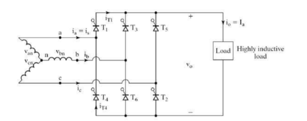
Figure Three phase full bridge
At ωt= (∏/6 +α), thyristor is already conducting when the thyristor is turned on by applying the gating signal to the gate of. During the time period ωt= (∏/6 +α) to (∏/2 +α), thyristors and conduct together and the line-to-line supply voltage appears across the load. At ωt= (∏/2 +α), the thyristor T2 is triggered and T6 is reverse biased immediately and T6 turns off due to natural commutation. During the time period ωt= (∏/ +α) to (5∏/6 +α), thyristor T1 and T2 conduct together and the line-to-line supply voltage appears across the load. The thyristors are numbered in the circuit diagram corresponding to the order in which they are triggered. The trigger sequence (firing sequence) of the thyristors is 12, 23, 34, 45, 56, 61, 12, 23, and so on. The figure shows the waveforms of three phase input supply voltages, output voltage, the thyristor current through T1 and T4, the supply current through the line ‘a’.
We define three-line neutral voltages as follows:
VRN = Van = Vm sin wt where Vm is the maximum voltage
VYN = Vbn = Vm sin (wt - 2π/3)
VBN – Vcn – Vm sin (wt - 4π/3)
The corresponding line to line voltages are
VRY = Vab = Van – Vbn = √3 Vm sin (wt + π/6)
VYB = Vbc = Vbn – Vcn = √3 Vm sin (wt - π/2)
VBR = Vca = Vcn – Van = √3 Vm sin (wt + π/2)
Q5) Explain three phase full bridge rectifier ?
A5) Three phase full converter is a fully controlled bridge controlled rectifier using six thyristors connected in the form of full wave bridge configuration. All the six thyristors are controlled switches which are turned on at an appropriate time by applying suitable gate trigger signals. The three- phase full converter is extensively used in industrial power applications up to about 120kW output power level, where two quadrant operation is required. The figure shows a three-phase full converter with highly inductive load. This circuit is also known as three phase full wave bridge or as a six-pulse converter.
The thyristors are triggered at an interval of (π/3) radians. The frequency of output ripple voltages is 6fs and the filtering requirement is less than that of three phase semi and half wave converters.
At wt=(π/6+ ) thyristor T6 is conducting when the thyristor T1 is turned on by applying the gating signal to the gate of T1. During the time period wt = =(π/6+
 ) to (=(π/2+
 ) thyristors T1 and T6 conduct together and the line-to-line supply voltage ab v appears across the load.
At wt = (π/2 + α) the thyristor T2 is triggered and T6 is reverse biased immediately and T6 turns off due to natural commutation. During the time period wt = (π/2 + α) to (5π/6 +α) together and the line-to-line supply voltage ac v appears across the load.
At wt = (π/6 + α) thyristors T6 is already conducting when the thyristor T1 is turned on by diagram corresponding to the order in which they are triggered. The trigger sequence (firing sequence) of the thyristors is 12, 23, 34, 45, 56, 61, 12, 23, and so on. The figure shows the waveforms of three phase input supply voltages, output voltage, the thyristor current through T1 and T4, the supply current through the line ‘a’
We define three-line neutral voltages (3 phase voltages) as follows
vRN = van = Vm sin wt
Vm = max phase voltage
vYN = vbn = Vm sin (wt - 2π/3) = Vm sin (wt -120 o)
v BN = vcn = Vm sin (wt + 2π/3) = Vm sin (wt + 120) = Vm sin (wt -240)
where Vm is the peak phase voltage of star Y connected source.
The corresponding line to line voltages are:
vRy = vab = (van – vbn) = √3 Vm sin (wt + π/6)
v YB = vbc = (vbm – vcn) = √3 Vm sin (wt – π/2)
v BR = vca = (vca – van) = √3 Vm sin (wt + π/2)
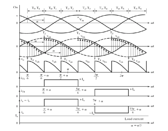
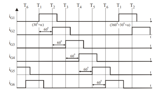
Figure . Output Waveform
Q6) Explain boost regulator?
A6) Boost regulator has been analyzed with a 3-φ diode bridge rectifier for the purpose of power factor correction. The circuit diagram of a typical Boost regulator is shown in figure 1. It consists of an inductor, a capacitor, a switch (IGBT) and a diode. Inductor is used as an energy storage element which has the tendency to resist the changes in current. When being charged it acts as a load and absorbs energy, when being discharged it acts as an energy source. The voltage it produces during the discharge phase is related to the rate of change of current, and not to the original charging voltage, thus allowing different input and output voltages. Capacitor C is used for filtering purposes. Boost regulator has been analyzed with a 3-φ diode bridge rectifier for the purpose of power factor correction. The circuit diagram of a typical Boost regulator is shown in figure 1. It consists of an inductor, a capacitor, a switch (IGBT) and a diode. Inductor is used as an energy storage element which has the tendency to resist the changes in current. When being charged it acts as a load and absorbs energy, when being discharged it acts as an energy source. The voltage it produces during the discharge phase is related to the rate of change of current, and not to the original charging thus allowing different input and output voltages. Capacitor C is used for filtering purposes. During high switching pulses switch gets turned on, the power flows from input side to the load side. At this time current through the inductors start rising linearly and it gets stored. The resulting output voltage is in positive phase of the input voltage. The mathematical expressions in these modes are voltage, thus allowing different input and output voltages. Capacitor C is used for filtering purposes. During high switching pulses switch gets turned on, the power flows from input side to the load side. At this time current through the inductors start rising linearly and it gets stored.
Q7) Explain its output voltage?
A7) The resulting output voltage is in positive phase of the input voltage. The mathematical expressions in these modes are
Vin = VL = L dI/ton
Vin ton = L dI
During low state of switching pulse switch gets turned off and inductor released its stored energy to the load through diode and bypass capacitor C. It is a continuous conduction process and power flow bidirectionally.
Q8) Design a circuit to produce an average voltage of 40V across a 100Ω load resistor from 120 Vrms 60 Hz ac source. Determine the power absorbed by the resistance and the power factor.
A8) Vdc = Vm/ 2 π( 1+cos α)
So α = cos-1 [ Vo(2π/Vm) -1]
= cos -1 { 40 [ 2π/ √2 (120) ] -1 } = 61.2 o = 1.07 rad.
Vrms = Vm/2 √ 1 -1.07/ π + sin[2(1.07)]/ 2π = 75.6 V
PR= V2 rms / R = (75.6) 2 / 00 = 57.1 W
Irms = Vrms/R = 75.6/100 = 0.756A
Pf = PR/S = 57.1/90.72 =0.629
Q9) Explain applications of single- phase half wave rectifier?
A9)
Q10) Explain phase controlled rectifier?
A10) The term PCR or Phase controlled rectifier is a one type of rectifier circuit in which the diodes are switched by Thyristors or SCRs. The term PCR or Phase controlled rectifier is a one type of rectifier circuit in which the diodes are switched by thyristors or SCRs. Whereas the diodes offer no control over the o/p voltage, the Thyristors can be used to differ the output voltage by adjusting the firing angle or delay. A phase control thyristor activated by a short pulse to its gate terminal and it is deactivated due to line communication or natural. In case of heavy inductive load, it is deactivated by firing another Thyristor of the rectifier during the negative half cycle of i/p voltage.SCRs whereas the diodes offer no control over the o/p voltage, the Thyristors can be used to differ the output voltage by adjusting the firing angle or delay.