Unit - 2
Combinational Logic Design
Q1) Convert the Boolean function into Standard SoP form.
f = p’qr + pq’r + pqr’ + pqr
A1)
Step 1 – By using the Boolean postulate, x + x = x and also writing the last term pqr two more times we get
⇒ f = p’qr + pq’r + pqr’ + pqr + pqr + pqr
Step 2 – By Using Distributive law for 1st and 4th terms, 2nd and 5th terms, 3rdand 6th terms.
⇒ f = qr (p’ + p) + pr (q’ + q) + pq (r’ + r)
Step 3 – Then Using Boolean postulate, x + x’ = 1 we get
⇒ f = qr (1) + pr (1) + pq (1)
Step 4 – hence using Boolean postulate, x.1 = x we get
⇒ f = qr + pr + pq
⇒ f = pq + qr + pr
This is the required Boolean function.
Q2) Convert the Boolean function into Standard PoS form.
f = (p + q + r). (p + q + r’). (p + q’ + r). (p’ + q + r)
A2)
Step 1 – By using the Boolean postulate, x.x = x and writing the first term p+q+r two more times we get
⇒ f = (p + q + r). (p + q + r). (p + q + r). (p + q + r’). (p +q’ + r). (p’ + q + r)
Step 2 – Now by using Distributive law, x + (y.z) = (x + y). (x + z) for 1st and 4thparenthesis, 2nd and 5th parenthesis, 3rd and 6th parenthesis.
⇒ f = (p + q + rr’). (p + r + qq’). (q + r + pp’)
Step 3 − Applying Boolean postulate, x.x’=0 for simplifying of the terms present in each parenthesis.
⇒ f = (p + q + 0). (p + r + 0). (q + r + 0)
Step 4 − Using Boolean postulate, x + 0 = x we get
⇒ f = (p + q). (p + r). (q + r)
⇒ f = (p + q). (q + r). (p + r)
This is the simplified Boolean function.
Hence, both Standard SoP and Standard PoS forms are Dual to one another.
Q3) What is a combinational circuit?
A3) A Combinational circuit is a circuit in which we combine the different gates. For example, encoder, decoder, multiplexer, demultiplexer etc. Some of the characteristics are as follows −
Block diagram
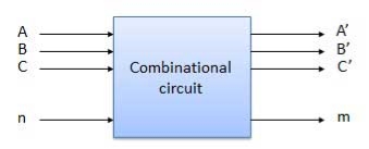
Fig. 1: Combinational circuit (ref.2)
Q4) Simplify f (X, Y, Z) =∏M (0,1,2,4) f (X, Y, Z) =∏M (0,1,2,4) using K-map.
A4)

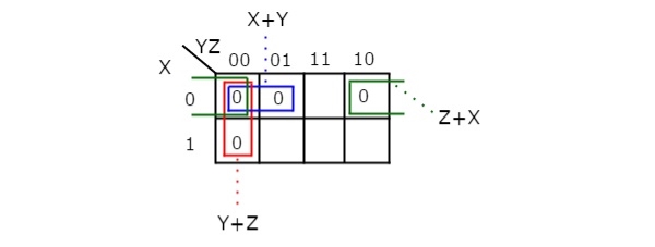
Therefore, the simplified Boolean function is
f = (X + Y). (Y + Z). (Z + X)
Q5) Simplify: F (P, Q, R, S) =∑ (0,2,5,7,8,10,13,15)
A5)

F = P’Q’R’S’ + PQ’R’S’ + P’Q’RS’ +PQ’RS’ + QS
F = P’Q’S’ + PQ’S’ + QS
F = Q’S’ +QS
Q6) Simplify: F (A, B, C) =π (0,3,6,7)
A6)

F = A’BC +ABC +A’B’C’ +ABC’
F = BC + C’ (A’B’ + AB)
Q7) Explain half adder with truth table and logic diagram?
A7)
Block diagram
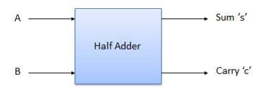
Fig.2: Half adder (ref. 2)
Truth Table
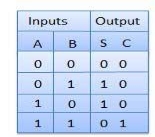
Circuit Diagram
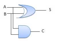
Fig.3: Half adder
Q8) Explain 4-bit parallel adder?
A8)
Block diagram
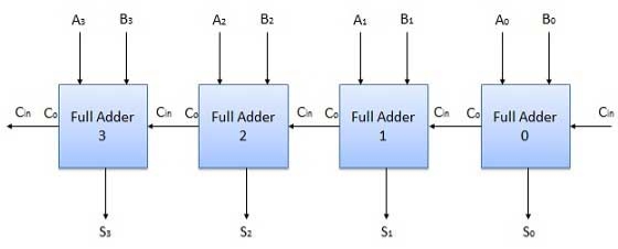
Fig.4: 4-bit parallel adder
Q9) Explain the internal diagram of look ahead carry adder?
A 9) In this, for each adder block, the two bits that are to be added are available instantly.

Fig 5: Look ahead Carry adder (ref. 2)

Fig.6: Look ahead Carry adder (ref. 2)

Q10) What are line decoders explain?
A10)
Truth Table –
X | Y | Z | D0 | D1 | D2 | D3 | D4 | D5 | D6 | D7 |
0 | 0 | 0 | 1 | 0 | 0 | 0 | 0 | 0 | 0 | 0 |
0 | 0 | 1 | 0 | 1 | 0 | 0 | 0 | 0 | 0 | 0 |
0 | 1 | 0 | 0 | 0 | 1 | 0 | 0 | 0 | 0 | 0 |
0 | 1 | 1 | 0 | 0 | 0 | 1 | 0 | 0 | 0 | 0 |
1 | 0 | 0 | 0 | 0 | 0 | 0 | 1 | 0 | 0 | 0 |
1 | 0 | 1 | 0 | 0 | 0 | 0 | 0 | 1 | 0 | 0 |
1 | 1 | 0 | 0 | 0 | 0 | 0 | 0 | 0 | 1 | 0 |
1 | 1 | 1 | 0 | 0 | 0 | 0 | 0 | 0 | 0 | 1 |
Implementation
D0 is high when X = 0, Y = 0 and Z = 0. Hence,
D0 = X’ Y’ Z’
Similarly,
D1 = X’ Y’ Z
D2 = X’ Y Z’
D3 = X’ Y Z
D4 = X Y’ Z’
D5 = X Y’ Z
D6 = X Y Z’
D7 = X Y Z
Hence,
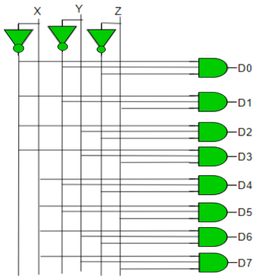
Fig 7 Decoder
Q11) Explain the implementation of encoder?
A11)
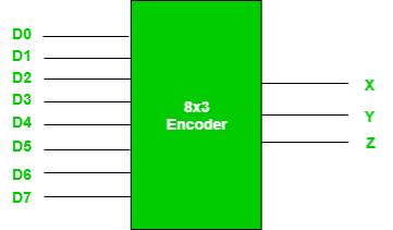
Fig.8: 8X3 Encoder (ref. 2)
Truth Table –
D7 | D6 | D5 | D4 | D3 | D2 | D1 | D0 | X | Y | Z |
0 | 0 | 0 | 0 | 0 | 0 | 0 | 1 | 0 | 0 | 0 |
0 | 0 | 0 | 0 | 0 | 0 | 1 | 0 | 0 | 0 | 1 |
0 | 0 | 0 | 0 | 0 | 1 | 0 | 0 | 0 | 1 | 0 |
0 | 0 | 0 | 0 | 1 | 0 | 0 | 0 | 0 | 1 | 1 |
0 | 0 | 0 | 1 | 0 | 0 | 0 | 0 | 1 | 0 | 0 |
0 | 0 | 1 | 0 | 0 | 0 | 0 | 0 | 1 | 0 | 1 |
0 | 1 | 0 | 0 | 0 | 0 | 0 | 0 | 1 | 1 | 0 |
1 | 0 | 0 | 0 | 0 | 0 | 0 | 0 | 1 | 1 | 1 |
Implementation –
X = D4 + D5 + D6 + D7
Y = D2 +D3 + D6 + D7
Z = D1 + D3 + D5 + D7
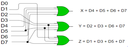
Fig 9: 8:3 encoder
Limitation of the encoder is that only one input is active at a time.
Q12) Explain the logic diagram of multiplexer?
A12)

Fig 10: Block diagram of multiplexer (ref. 2)
Multiplexers come in multiple variations
Block Diagram of 2:1 MUX
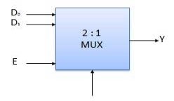
Truth Table of 2:1 MUX

Where x is don’t care.
Q13) What are demultiplexers?
A13)
Various Demultiplexers are used as:
Block diagram
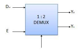
Truth Table

Where x is don’t care.
Q14) Realize all the logic gates using NAND gate?
A14) Implementing an inverter using NAND gate
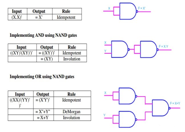

Fig 11 Implementation of basic gates using NAND gate
Q15) Realize logic gates using NOR gate?
A15)
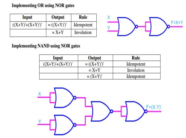
Fig 12 Implementation of Or and NAND gate using NOR gate