Unit - 3
Synchronous Sequential logic Design
Q1) What are sequential circuits?
A1)

Fig. 1 Combinational circuit

Fig. 2 Sequential circuit
There are two types of input to the combinational logic in fig 2:
Secondary inputs are state variables that are produced by the storage elements whereas secondary outputs are excitations for those storage elements.
Q2) What are the types of sequential circuits?
A2) There are two types of sequential circuit:

Fig. 3 Asynchronous Sequential circuit
But they are more difficult to design and their output is also uncertain.

Fig. 4 Synchronous Sequential circuit
Q3) Write truth table for SR latch?
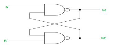
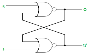
A3) SR Latch is a circuit which has:
(i) 2 cross-coupled NOR gate or NAND gate.
(ii) 2 input S for SET and R for RESET.
(iii) 2 output Q and Q’.
Q | Q’ | STATE |
1 | 0 | Set |
0 | 1 | Reset |
Under normal conditions, both the input remains 0.
RS Latch with NAND gates:
Case-1: When S’=R’=1 or S=R=0 then
If Q = 1, Q = R’ = 1.
If Q = 0, Q = 0 and R’ = 1 respectively.
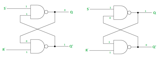
Case-2: S’=0, R’=1 (S=1, R=0)
As S’=0, Q = 1(SET state).
In 2nd NAND gate, as Q = R’ = 1, Q’=0.
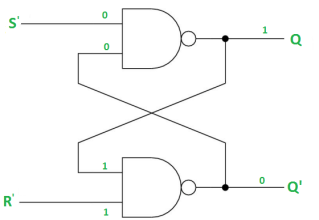
Case-3: S’= 1, R’= 0 (S=0, R=1)
As R’=0, Q’ = 1.
In 1st NAND gate, as Q =S’ = 1, Q=0 (RESET state).
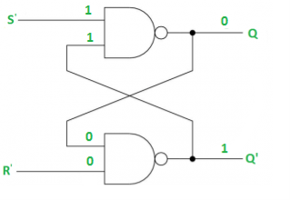
Case-4: S’= R’= 0 (S=R=1)
When S=R=1, both Q = Q’ = 1 which is not allowed.
So, this input condition is prohibited.
The SR Latch using NOR gate is:
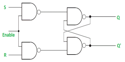
Q4) Explain the gated SR latch with circuit diagram?
A4) It is a latch which enable input that works when enable = 1 and retain the previous state when enable = 0.
Q5) Using NAND gates explain the gated D latch?
A5) It is similar to SR latch with little modifications. Here, the inputs are complements of one another. The design of D latch with Enable signal is given below:
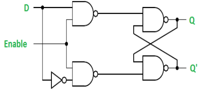
The truth table is shown below:
ENABLE | D | Q(N) | Q(N+1) | STATE |
1 | 0 | x | 0 | RESET |
1 | 1 | x | 1 | SET |
0 | x | x | Q(n) | No Change |
As the output is same as input, it is also known as Transparent Latch.
The characteristic equation for D latch with enables input is given as:
Q(n+1) = EN. D + EN’. Q(n)
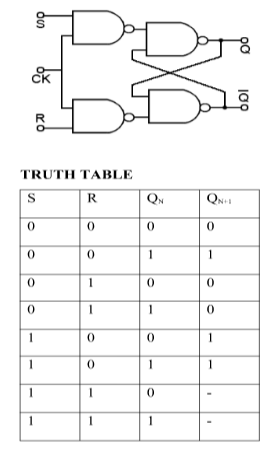
Q6) Explain SR flip flop with logic diagram and truth table?
A6) S-R Flip Flop:
Q7) Explain the truth table and logic diagram of JK flip flop?
A7) J-K Flip Flop:

Q8) Explain the truth table and logic diagram of D flip flop?
A8) D Flip Flop:


Q9) Explain the truth table and logic diagram of T flip flop?
A9)


Q10) What is race around condition?
A10) Race Around Condition in JK Flip-flop –
Q11) How can we overcome the race around condition in JK flip flop?
A11) Master Slave JK flip flop –

Fig. 5 Master Slave Flip flop
Working of a master slave flip flop –
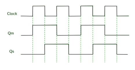
Q12) Explain the timing diagram of Master Slave JK flip flop?
A12) Timing Diagram of a Master flip flop –
Q13) What are state table and state diagrams in flip flops?
A13) State Table
The state table representation of a sequential circuit consists of three sections labeled present state, next state and output. The present state designates the state of flip-flops before the occurrence of a clock pulse. The next state shows the states of flip-flops after the clock pulse, and the output section lists the value of the output variables during the present state.
State Diagram
In addition to graphical symbols, tables or equations, flip-flops can also be represented graphically by a state diagram. In this diagram, a state is represented by a circle, and the transition between states is indicated by directed lines (or arcs) connecting the circles.

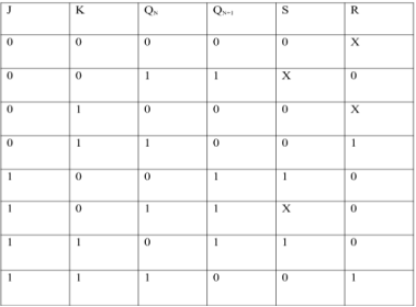
Q14) Convert SR to JK flip flop write the conversion table?
A14) SR To JK Flipflop
Excitation Functions:

Q15) Write the excitation table for conversion of SR to D flip flop?
A15) Convert SR to D Flip-Flop:

Excitation Functions:
S = D
R = D ‘


