Unit - 4
Binary Counter
Q1) Mention the difference between Mealy machine and Moore Machine?
A1) The following table highlights the points that differentiate a Mealy Machine from a Moore Machine.
Mealy Machine | Moore Machine |
Output depends both upon the present state and the present input | Output depends only upon the present state. |
Generally, it has fewer states than Moore Machine. | Generally, it has more states than Mealy Machine. |
The value of the output function is a function of the transitions and the changes, when the input logic on the present state is done. | The value of the output function is a function of the current state and the changes at the clock edges, whenever state changes occur. |
Mealy machines react faster to inputs. They generally react in the same clock cycle. | In Moore machines, more logic is required to decode the outputs resulting in more circuit delays. They generally react one clock cycle later. |
Q2) A four bit modulo 16 ripple counter uses JK flip flops. If the propagation delay of each flip flop is 50ns, find the maximum clock frequency that can be used?
A2) Propagation delay of each flip flop = 50ns
Four bit modulo 16 ripple counter represents n=4
Maximum clock frequency =  =
=  = 5MHz
Q3) A pulse train with a frequency of 1MHzis counted using a modulo-1024 ripple counter built with JK flip flop. Find the maximum permissible propagation delay/flip flop for proper operation of the counter?
A3) f= 1MHz
T= 1000ns
Mod-1024= 2n
210=2n
n=10
Propagation delay for one flip flop Td = T/n = 1000x 10-9/10
Td=100ns
Q4) If a counter having 10 flip flops is initially 0. Find the count it will hold after 2060 pulses?
A4) As counter has 10 flip-flops.
Hence, it counts from (0)10-(1023)10. So, total it has 1024 states.
2060-1024 = 1036
1036-1024 = 12
So, the value of counter after 2060 pulses is same that after 12 pulses given as 1100
(12)10 = (1100)2
So, after 2060 pulses the count will be (1100)2
Q5) A certain JK flip flop has tpd =12ns. Find the largest MOD counter that can be constructed from such flip flops and still operate up to 10MHz?
A5) Output frequency fout = 
10x106=
n=8bits
The given counter has 8-bits. It can have maximum count of 256. So, we can construct MOD-256 counter with given information.
Q6) A switch trail ring counter is made by using a single D flip flop. What will be the resulting circuit?
A6) In a switch trail ring counter is made by using a single D flip flop, the complementary output  is connected to D then it becomes T flip flop.
Q7) Explain the pin configuration of 7490?
A7) This is basically a decade counter which counts upwards on applying the clock signal. It consists of four master-slave JK flip flops as divide by 2 and divide by 5 counters in it. It can store decimal digits in 4-bit binary numbers. The divide by 2 and divide by 5 counters can be used individually each by disabling the other or both simultaneously to produce MOD-10 counter.

Fig: Pin Diagram of 7490
The pin configuration is explained below.
Pin1: clock input 2
Pin2: reset1
Pin3: reset2
Pin3: Not connected
Pin4: Supply voltage
Pin5: reset3
Pin6: reset4
Pin8: BCD output bit 2 (Qc)
Pin9: BCD output bit 1 (Qb)
Pin10: ground
Pin11: BCD output bit 3 (QD)
Pin12: BCD output bit 0 (QA)
Pin13: Not connected
Pin14: clock input 1
It is 4-bit binary decade counter with four outputs QA, QB, QC, QD. After the count value reaches 10 the binary output is reset. The MOD of this IC can be changed by the reset pins R0(1), R0(2), R9(1) and R9(2). If R0(1), R0(2) is high or R9(1) and R9(2) are ground the four outputs QA, QB, QC, QD are reset to 0000.
Q8) Implement BCD decade counter using 7490?
A8) The push button switch SW1 when released eery time will increase the count value by one. When the count due to SW1 reaches 1001 the outputs QA, QB, QC, QD are reset to 0000.

Truth table is as follows:
Clock pulse | Q3 | Q2 | Q1 | Q0 |
0 | 0 | 0 | 0 | 0 |
1 | 0 | 0 | 0 | 1 |
2 | 0 | 0 | 1 | 0 |
3 | 0 | 0 | 1 | 1 |
4 | 0 | 1 | 0 | 0 |
5 | 0 | 1 | 0 | 1 |
6 | 0 | 1 | 1 | 0 |
7 | 0 | 1 | 1 | 1 |
8 | 1 | 0 | 0 | 0 |
9 | 1 | 0 | 0 | 1 |
10 | 0 | 0 | 0 | 0 |
Q9) Explain the internal structure and pin configuration of IC 7474?
A9)

Pin 1, Clear 1 Input
Pin 2, D1 input
Pin 3, Clock 1 Input
Pin 4, Preset 1 Input
Pin 5, Q1 output
Pin 6, Complement Q1 output
Pin 7, Ground
Pin 8, Complement Q2 output
Pin 9, Q2 output
Pin 10, Preset 2 Input
Pin 11, Clock 2 Input
Pin 12, D2 input
Pin 13, Clear 2 Input
Pin 14, Positive Supply
It is basically a dual D type edge triggered flip flop. The input is high on the positive edge of clock pulse. When the clock pulse is low or high the data in the D flip flop can be changed without changing the output. The input is reset when there is LOW logic level at the preset.
The value stored at particular value of clock cycle becomes the output. After that for different time the value of output does not change. It is widely used in data storage.
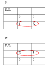
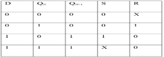
Q10) Convert SR to D flip flop?
A10)
Excitation Functions:
S = D
R = D ‘


Q11) List the differences between asynchronous and synchronous counters?
A11)
| Asynchronous | Synchronous |
1 | The flip flops are connected in such a way that the output of the first drives the clock for the second, the output of the second drives the third and so on. | 1 There is no connection between the output of first and clock of second flip flop.
|
2 | All flip flops are not clocked simultaneously. | 2 All flip flops are clocked simultaneously |
3 | Design and implementation are simple. | 3 Design becomes difficult if number of states increased. |
4 | Low speed | 4 High speed |
Q12) Explain Master slave flip flop?
A12)

Fig. Master-Slave Flip flop
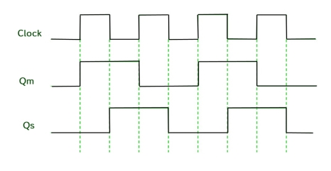
Working of a master-slave flip flop –
Timing Diagram of a Master flip flop –

