UNIT 5
CONDENSED MATTER AND MATERIAL
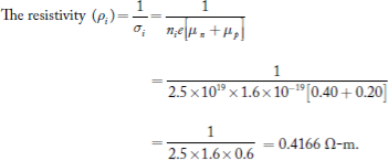
1 Question: Find the resistivity of an intrinsic semiconductor with intrinsic concentration of 2.5 × 10¹⁹ per m3. The mobilities of electrons and holes are 0.40 m2/ V-s and 0.20 m2/ V-s.
Solution:
Given data are:
Intrinsic concentration (ni) = 2.5 × 10¹⁹/m3
Mobility of electrons (μn) = 0.40 m2/V-s
The mobility of holes (μp) = 0.20 m2/V-s
The conductivity of an intrinsic semiconductor (σi) = nie[μn + μp]
2 Question: Define the term Space Lattice?
Solution:
In a solid crystalline material, the atoms or molecules are arranged regularly and periodically in all three dimensions. The atomic arrangement in a crystal is called crystal structure.
To explain crystal symmetries easily, it is convenient to represent an atom or a group of atoms that repeats in three dimensions in the crystal as a unit. If each such atom or unit of atoms in a crystal is replaced by a point in space, then the resultant points in space are called space lattice.
Each point in a space lattice is called a lattice point. Each atom or unit of atoms is called basis or pattern.
A space lattice represents the geometrical pattern of crystal in which the surroundings of each lattice point is the same. If the surroundings of each lattice point is same or if the atom or all the atoms at lattice points are identical, then such a lattice is called Bravais lattice.
On the other hand, if the atom or the atoms at lattice points are not same, then it is said to be a non-Bravais lattice.
A space lattice or crystal lattice is defined as three dimensional infinite arrays of points in space in which every point has surroundings identical to that of every other point in the array.
3 Question: Define Basis in Crystal Structure?
Solution:
The atomic arrangement in a crystal is called crystal structure. The crystal structure is formed by associating every lattice point with an atom or an assembly of atoms or molecules or ions, which are identical in composition, arrangement and orientation, called the basis. i.e. an atom, or a group of atoms or molecules identical in composition is called the basis or the pattern.
The basis provides the number of atoms per lattice point, their types, mutual orientations and distances of separation between the atoms.
If the basis is substituted for the lattice points, then the resulting structure is called crystal structure as shown in Figure.
Lattice + basis = crystal structure.
The basis shown in Figure contains two different atoms. In copper and sodium crystals the basis is single atoms; In NaCl, the basis is diatomic and in CaF2 the basis is triatomic. A lattice is an imaginary assumption while the crystal structure is a real concept.

1 Figure: Lattice sites, Basis and crystal structure
4 Question: What is Unit Cell and also discuss about Lattice Parameters?
Solution:
Unit cell
Unit cell is small repeating entity of the atomic structure. It is the basic building block of the crystal structure. It defines the entire crystal structure with the atom positions within.
Unit cells for most of the crystals are parallelepipeds or cubes having three sets of parallel faces. A unit cell is the basic structural unit or building block of the crystal.
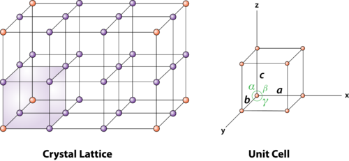
2 Figure: unit cell and unit cell parameter
A unit cell is defined as the smallest parallelepiped volume in the crystal, which on repetition along the crystallographic axes gives the actual crystal structure or the smallest geometric figure, which on repetition in three-dimensional space, gives the actual crystal structure is called a unit cell.
Choice of a unit cell is not unique but it can be constructed in a number of ways as shown in figure. Following figure shows different ways of representing unit cells in a two-dimensional lattice. A unit cell can be represented as ABCD or A′B′C′D′ or A′′B′′C′′D′′, etc.
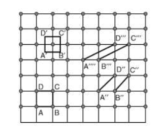
3 Figure: Construction of unit cell in different way
First we define crystallographic axes. These axes are obtained by the intersection of the three non-coplanar faces of the unit cell. The angles between these faces or crystallographic axes are known as interfacial or interaxial angles. The angles between the axes Y and Z is α, between Z and X is β and between X and Y is γ. The translational vectors or primitives a, b, c of a unit cell along X, Y, Z axes and interaxial angles α, β, γ are called Cell parameters. These cell parameters are shown in (Figure 2). The cell parameters determine the actual size and shape of the unit cell.
5 Question: What do you meant by Primitive and non-primitive unit cells?
Solution:
The unit cell formed by primitives is called a simple or a primitive unit cell. A primitive unit cell contains only one lattice point. If a unit cell contains more than one lattice point, then it is called a non-primitive unit cell or a multiple unit cell. Most of the unit cells of various crystal lattices contain two or more lattice points and hence it is not necessary that unit cell should be a primitive unit cell.
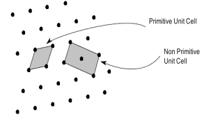
4 Figure: Primitive and non-primitive unit cells
6 Question: What is the Difference between Crystalline solids and amorphous solids?
Solution:
Crystalline solids | Amorphous solids |
|
|
2. They have long range order of regular pattern of arrangement of constituent particles. | 2. They have short range order of regular pattern of arrangement of constituent particles. |
3. They are true solids. | 3. They are pseudo solids or super cooled |
4. They have sharp melting points. | 4. They do not have sharp melting points. |
5. They are anisotropic in nature. | 5. They are isotropic in nature. |
6. They have definite heat of fusion. | 6. They do not have definite heat of fusion. |
7 Question: What are the major differences between type I and Type II superconductor?
Solution:
Differences between type I and Type II superconductor
Type I superconductor | Type II superconductor |
1. It follows complete Meissner effect. | 1. It does not follow the complete Meissner effect |
2. It has single critical field value HC | 2. It has two critical field values HC1 and HC2. |
3. There no mixed state. | 3. There is a mixed state |
4. They are soft superconductors | 4. They are hard superconductors |
5. Materials with pure form are type I superconductors | 5. Materials with impurities or alloys are type II superconductors |
8 Question: Define superconductivity. Also discuss properties of superconductors?
Solution:
Superconductivity
The ability of certain metals, their compounds and alloys to conduct electricity with zero resistance at very low temperature is called superconductivity. The materials which exhibit this property are called superconductors.
Properties
Following properties are shown by superconductors.
- It is a low temperature phenomenon.
- The electrical resistivity drops to zero.
- The conductivity becomes infinity.
- The transition temperature is different for different substances.
- Material having high normal resistivity exhibit superconductivity.
- Materials for which ρZ= 106 (where Z is a atomic number and ρ is resistivity) show superconductivity.
- Superconductivity is very sharp for chemically pure and structurally perfect specimen.
- Ferro magnetic and Anti ferromagnetic materials are not superconductors.
- Below the transition temperature the magnetic flux lines are rejected out of the superconductors.
- Generally Superconducting elements lie in the inner columns of the periodic table.
- Those metallic elements having their valence electrons lies between 2 to 8 exhibit superconductivity.
- Below the transition temperature the specific heat curve is discontinuous.
- There is a discontinuous change in specific heat.
- There are small changes in volume and thermal conductivity of the material.
9 Question Prove that susceptibility of superconductor is -1 and relative permeability is zero.
Solution:
We know Induced Magnetic Field B = μ0(H+M)
Where H is the external applied magnetic field and M is the magnetization produced inside the specimen.
When the specimen is in superconducting state B=0 (Meissner effect)
B = μ0(H+M)
0 = μ0(H+M)
H= -M
χ = H/M = -1
Thus the material is act as a perfectly diamagnetic because for diamagnetic material susceptibility χ = -1
Also χ = μr -1
μr = -1+1 =0
Hence proved susceptibility of superconductor is -1 and relative permeability is zero.
10 Question: Discuss various applications of Superconductors?
Solution:
Applications of Superconductors
- Superconductors form the basis of energy saving power systems, namely the superconducting generators, which are smaller in size and weight, in comparison with conventional generators.
- Superconducting magnets have been used to levitate trains above its rails. They can be driven at high speed with minimal expenditure of energy.
- Superconducting magnetic propulsion systems may be used to launch satellites into orbits directly from the earth without the use of rockets.
- High-efficiency ore-separating machines may be built using superconducting magnets which can be used to separate tumour cells from healthy cells by high gradient magnetic separation method.
- Since the current in a superconducting wire can flow without any change in magnitude, it can be used for transmission lines.
- Superconductors can be used as memory or storage elements in computers.
11 Question : Distinguish between conductor, insulator and semiconductor?
Or
Discuss band theory of solids?
Solution:
We can distinguish between conductor, insulator and semiconductor by the Band Model
Bands are formed by the closely spaced orbitals.
There are three types of bands:
1. Valance Bands: Valence band it is a group of orbitals which contain electrons in the shell. Or we can say It is also defined as the energy band that comprises of valence electrons present in the outermost shell of an atomic structure.
These valence electrons, when provided with sufficient energy, get changed into free electrons and moves to conduction band thereby causing conductivity. It is at a lower energy level than the conduction band in the energy level diagram.
2. Conduction Band: Conduction band is a group of empty orbitals of the shells that do not contain any electron due to their configuration making the orbitals of higher energy levels.
When the electrons pass from valance band to the conduction band these solids conduct electricity with flow of charges in the form of electrons.
3. Forbidden Energy Band: These two bands are separated by a certain amount of energy known as the forbidden energy gap. In this band not a single electron is available. It diagram it is named as Band Gap.
Let us distinguish between conductor, semiconductors and insulator on the basis of these bands.
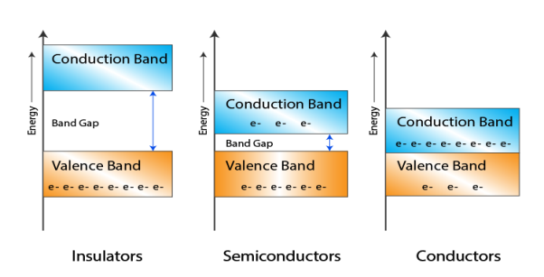
- In Conductors: The valance band and the conduction band overlap each other. This makes it easy for the electricity to pass through them. In conductors, the valence band is either not fully occupied with electrons, or the filled valence band overlaps with the empty conduction band. In general, both states occur at the same time, the electrons can therefore move inside the partially filled valence band or inside the two overlapping bands. In conductors there is no band gap between the valence band and conduction band.
- In Semi-conductors: there is a slight gap between the conduction band and the valance band. This band gap is less than or equal to 1.4 eV. The electrons from valance shell take a little energy to excite from valance band to the conduction band. Even in semiconductors, there is a band gap, but compared to insulators it is so small that even at room temperature electrons from the valence band can be lifted into the conduction band. The electrons can move freely and act as charge carriers.
- In Insulators: In insulators the valence band is fully occupied with electrons due to the covalent bonds. To achieve conductivity, electrons from the valence band have to move into the conduction band. the energy gap is considerably large and the electrons of the valance band cannot be excited to the conduction band before the melting or the dissociation of the solid. This means that under the practically ambient condition it cannot conduct electricity.
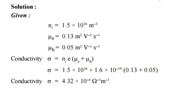
12 Question The intrinsic carrier density is 1.5 × 10¹⁶ m–3. If the mobility of electron and hole are 0.13 and 0.05 m2 V–1 s–1, calculate the conductivity.
13. Question: Write Properties of X-rays?
Solution:
- X-rays are electromagnetic waves having a wavelength in the range from 1 Å to 100 Å.
- X-rays are high energetic waves as compared to visible light, UV, infrared radiations, microwaves and radio waves.
- They have a shorter wavelength of the electromagnetic spectrum.
- X-rays can ionize atoms and molecules of matter.
- They travel by a velocity of light i.e. 3 x10⁸ ms-1 in vacuum or air.
- They are not deflected by magnetic or electric fields and, therefore, do not possess any charge.
- X-ray can produce the photoelectric effect.
- X-rays can affect photographic plates.
- X-rays can ionize a gas through which they pass.
- X-rays can be made to reflect, refract and diffract. X-rays show the phenomenon of interference and polarization.
- X-rays can produce fluorescence in certain metal.
- When certain x-rays fall on certain metals, secondary X-rays are produced.
- They show particle-like properties in interacting with matter as in photoelectric effect and Compton Effect.
- Frequency = 3×10¹⁶ to 3×10¹⁹ Hz
- Energy = 0.1 to 100 keV
- Requires high voltage to produce X-Rays.
- They are capable of travelling in a vacuum.
- They are pure energy.
- They can penetrate various objects.
- They induce colour changes of Methylene and sodium platinocyanide.
- They cause destruction of fermenting power of enzymes.
14. Question: How X ray can be Produced?
Solution:
A current is passed through the tungsten filament and heats it up. As it is heated up the increased energy enables electrons to be released from the filament through thermionic emission. The electrons are attracted towards the positively charged anode and hit the tungsten target with a maximum energy determined by the tube potential i.e. voltage. As the electrons bombard the target they interact via Bremsstrahlung and characteristic interactions which result in the conversion of energy into heat (99%) and x-ray photons (1%).
The x-ray photons are released in a beam with a range of energies out of the window of the tube and form the basis for x-ray image formation.
Production of X-rays When fast moving electrons strike on a very hard target of high atomic number like platinum, tungsten, molybdenum etc., X-rays are produced. Dr. William Collidge, in 1913, designed a tube for the production of X-rays. This tube is known as collidge tube or modern x-rays tube.
The Coolidge tube consists of a glass tube G exhausted to nearly, perfect vacuum of about -10-5 mm of mercury provided with a cathode and the target T. The cathode consists of a tungsten filament (F) heated by a low tension battery. Filament acts as cathode. It is made of thin (0.2 mm) tungsten wire. Since tungsten has a high atomic number (A 184, Z 74) so it is a good thermionic emitter i.e. good at emitting electrons. It has a very high melting temperature (3422°c). The size of the filament relates to the size of the focal spot. Some cathodes have two filaments for broad and fine focusing
The filament is placed inside a metal cup C to focus the electron on to the target. The target is made like tungsten or molybdenum having high melting point and high atomic weight held at an angle of 45° to the horizontal. The target T held by a copper rod outside the tube. The anode is connected to the positive and cathode to the negative terminal of the high tension power supply.
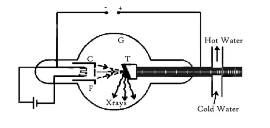
7 Figure: Coolidge X-ray Tube
Working
The filament F is heated by a passing a suitable current through it. The electrons emitted from the filament are focused at a point on the target with the help of a metal cup C. On account of the extremely high potential difference between the cathode and the anode, the electrons arrive at the target with high speed. The speed of the electrons can be further increased by increasing the accelerating voltage. On striking the anode, the electrons are stopped. Nearly 98% of the energy of the incident electrons is converted into heat. The remaining energy appears in the form of X-rays. However, intense heat is produced, which may melt the target. Therefore, the target must be cooled to remove the heat generated in it by continuous electron bombardment. The usual method is to mount the target material on the hollow copper tube through which cold water is continuously circulated.
Control of Intensity and Quality
Modern X-ray, the tube has the advantage of independent control of intensity and quality.
1 Control of intensity
The intensity of X-rays depends upon the number of electrons emitted from the filament. This depends upon the electric current flowing through the filament. So by controlling the current with the help of rheostat, we can control the intensity of X-rays. Hence, the intensity of the can be changed by adjusting the filament current.
2 Control of quality
If V be the potential difference applied across the two electrodes, then the kinetic energy acquired by the electron is given by
EV = 1/ 2mv2
Where m, e and v be the mass, charge and velocity of the electron.
Therefore, the quality of X-rays depends upon their energy which, in turn, depends upon the kinetic energy of the incident electrons. The kinetic energy of the incident electrons depends upon the potential difference between the anode and the cathode. Hence, quality of X-rays can be adjusted by changing the potential difference across the tube. X-rays having low penetrating power are called soft X-rays whereas X-rays having high penetrating power are called hard X-rays.
Frequency and Wavelength of X-rays Produced
When the whole of the kinetic energy of the electron is converted into the energy of the X-rays produced and then X-ray of maximum frequency is obtained. Therefore, if fmax is the maximum frequency of the emitted X-rays, then we have
Hfmax = eV = 1/ 2mv2
Where, h is a Planck's constant.
fmax = eV /h
If c is the velocity of light in vacuum and λmin be the minimum possible wavelength of the x-rays produced, then
λmin = C/ fmax =hc/eV
Nature of X-rays
X-rays are similar to light waves, but of much shorter wavelength about 0.1 nm. However, the wavelength of visible light is nearly 103 times more than the wavelength of X-rays. While the wavelength of the visible light ranges from 4000 Å to 8000 Å, the wavelength of X-rays generally lies between 1 to 3Å. Since wavelength is inversely proportional to frequency, therefore the frequency of X-rays is nearly 103 of visible light. Again, since the energy of the photon is directly proportional to frequency, therefore, x-ray photons are much stronger than the photons of visible light.
15. Question: Write Applications of X – Rays?
Solution:
X-rays are types of electromagnetic radiation probably most well-known for their ability to see through a person's skin and reveal images of the bones beneath it. Advances in technology have led to more powerful and focused X-ray beams as well as ever greater applications of these light waves from imaging teeny biological cells and structural components of materials like cement to killing cancer cells.
Most people are familiar with x-rays because of their use in medical imaging but there are many other applications of the radiation:
- In diagnostic medicine, x-rays are used to view bone structures, to detect the breakage in human bones.
- Hard x-radiation is used to minimize absorption of low energy x-rays. A filter is placed over the x-ray tube to prevent transmission of the lower energy radiation.
- The high atomic mass of calcium atoms in teeth and bones absorbs x-radiation, allowing most of the other radiation to pass through the body.
- Computer tomography (CT scans), fluoroscopy, and radiotherapy are other x-radiation diagnostic techniques.
- X-rays may also be used for therapeutic techniques, such as cancer treatments.
- X-rays are used for crystallography, astronomy, microscopy, industrial radiography, spectroscopy, fluorescence and to implode fission devices.
- X-rays may be used to create art and also to analyse paintings.
- Banned uses include x-ray hair removal and shoe-fitting fluoroscopes, which were both popular in the 1920s.
- They are used for medical purposes
- X-rays are used for airport security. They are used as a scanner to scan the luggage of passengers in airports, rail terminals, and other places.
- It is emitted by celestial objects and is studied to understand the environment.
- It is widely used to detect the defects in the welds.
16. Question: Define Fermi Energy and show its variation with temperature?
Solution:
It can be defined as:
The Fermi energy is a concept in quantum mechanics usually refers to the energy difference between the highest and lowest occupied single-particle states in a quantum system of non-interacting fermions at absolute zero temperature.
The value of the Fermi level at absolute zero temperature is known as the Fermi energy. It is also the maximum kinetic energy an electron can attain at 0K. Fermi energy is constant for each solid.
To determine the lowest possible Fermi energy of a system, we first group the states with equal energy into sets and arrange them in increasing order of energy. We then add particles one at a time, successively filling up the unoccupied quantum states with the lowest energy.
When all the particles are arranged accordingly, the energy of the highest occupied state is the Fermi energy.
In Spite of the extraction of all possible energy from metal by cooling it to near absolute zero temperature (0 Kelvin), the electrons in the metal still move around. The fastest ones move at a velocity corresponding to a kinetic energy equal to the Fermi energy.
The highest energy level that an electron can occupy at the absolute zero temperature is known as the Fermi Level. The Fermi level lies between the valence band and conduction band because at absolute zero temperature the electrons are all in the lowest energy state. Due to lack of sufficient energy at 0 Kelvin, the Fermi level can be considered as the sea of fermions (or electrons) above which no electrons exist. The Fermi level changes as the solids are warmed and as electrons are added to or withdrawn from the solid.
Don’t get confuse between Fermi level and Fermi energy. Both the terms are equal at absolute zero temperature but they are different at other temperature.
Fermi function F (E):
Fermi-Dirac distribution function represents the probability of an electron occupying a given energy level at absolute temperature. It is given by

Where KB Boltzmann Constant
T Temperature
Effect of temperature on Fermi Function:
Case (i) Probability of occupation for E < EF at T = 0K

When T = 0K and E < EF, we have
F(E) =  =
=  = 1
= 1
Thus at T = 0K, there is 100 % chance for the electrons to occupy the energy levels below the Fermi level.

10 Figure: Fermi distribution
Case (ii) Probability of occupation for E>EF at T = 0K
When T = 0K and E > EF, we have
F(E) =  =
=  =
=  = 0
= 0
Thus, there is 0 % chance for the electrons to occupy energy levels above the Fermi energy level. From the above two cases, at T = 0K the variation of F(E) for different energy values becomes a step function.
Case (iii) Probability of occupation at ordinary temperature
At ordinary temperature, the value of probability starts reducing from 1 for values of E slightly less than EF. With the increase of temperature, i.e., T> 0K, Fermi function F (E) varies with E.
At any temperature other than 0K and E = EF
F(E) =  =
=  =
=  = 50%
= 50%
Hence, there is 50 % chance for the electrons to occupy Fermi level. Further, for E > EF the probability value falls off rapidly to zero.
Case (iv) At high temperature
When kT >> EF, the electrons lose their quantum mechanical character and Fermi distribution function reduces to classical Boltzmann distribution.
17. Question: Derive Expression for the electrical conductivity and mobility?
Solution:
Electrical conductivity is defined as the rate of charge flow across unit area in a conductor per unit potential (voltage) gradient.
= 
Its unit is -1m-1 or Sm-1.
When an electrical field (E) is applied to an electron of charge ‘e’ of a metallic rod, the electron moves in opposite direction to the applied field with a velocity vd. This velocity is known as drift velocity.
Drift velocity vd is defined as the average velocity of the free electrons with which they move towards the positive terminal under the influence of the electrical field.
Lorentz force acting on the electron F = eE........(1)
This force is known as the driving force of the electron.
Due to this force, the electron gains acceleration ‘a’.
From Newton’s second law of motion,
Force F = ma…....(2)
From the equation (1) and (2),
Ma = eE or
a =  …......(3)
Acceleration (a) = 
Or a = 
Relaxation time is defined as the time taken by a free electron to reach its equilibrium position from the disturbed position in the presence of an electric field.
So vd = a……….(4)
Substituting equation (3) in (4)
vd =  =
=  E……….(5)
The Ohms’ law states that current density (J) is expressed as
J =E ……….(6)
Or = 
Where is the electrical conductivity of the electron.
But, the current density in terms of drift velocity is given as
J = nevd....... (7)
Substituting equation (5) in equation (7), we have
J = ne E
E
Or  =
= 
On comparing the equation (6) and (8) , we have
Electrical conductivity
=  ....... (8)
This is a required expression for electrical conductivity.
Mobility: It is defined as the drift velocity of the charge carrier per unit applied electric field.
μ=  ....... (9)
From equation (7) we have
J = nevd
By substituting vd =μE from equation (9)
J = neμE
Or  = μne....... (10)
We know by ohms law =  so equation (10) can be rewritten as
= μne
μ = 
This is the required expression for mobility.
18. Question: Derive hall coefficient? Show how hall coefficient and mobility are related?
Solution:
When magnetic field is applied perpendicular to a current-carrying conductor, then a voltage is developed in the material perpendicular to both magnetic field and current in the conductor. This effect is known as Hall Effect and the voltage developed is known as Hall voltage (VH).
Hall Effect is useful to identify the nature of charge carriers in a material and hence to decide whether the material is n-type semiconductor or p-type semiconductor, also to calculate carrier concentration and mobility of carriers.
Hall Effect can be explained by considering a rectangular block of an extrinsic semiconductor in which current is flowing along the positive X-direction and magnetic field B is applied along Z-direction as shown in Figure.
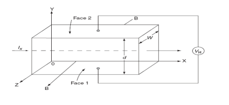
11 Figure: Hall Effect
Suppose if the semiconductor is n-type, then mostly the carriers are electrons and the electric current is due to the drifting of electrons along negative X-direction or if the semiconductor is p-type, then mostly the carriers are holes and the electric current is due to drifting of the holes along positive X-direction.
As these carriers are moving in magnetic field in the semiconductor that mean they experience Lorentz force represented by FL
FL = Bevd
Where vd is the drift velocity of the carriers. (already explained in previous section).
We can obtain the direction of this force by applying Fleming’s left-hand rule in electromagnetism.
Fleming’s left-hand rule can be explained as If we stretch the thumb, fore finger and middle finger in three perpendicular directions so that the fore finger is parallel to the magnetic field and the middle finger is parallel to the current direction, then thumb represents the direction of force on the current-carrying carriers.
So the Lorentz force is exerted on the carriers in the negative Y-direction. Due to Lorentz force, more and more carriers will be deposited at the bottom face (represented by face 1in figure) of the conductor.
The deposition of carriers at the bottom face is continued till the repulsive force due to accumulated charge balances the Lorentz force.
After some time of the applied voltage, both the forces become equal in magnitude and act in opposite direction, then the potential difference between the top and bottom faces is equal to Hall voltage and that can be measured.
At equilibrium, the Lorentz force on a carrier
FL = Bevd……………..(1)
And the Hall force
FH = eEH ……………..(2)
Where EH is the Hall electric field due to accumulated charge.
At equilibrium, FH = FL
EEH = Bevd
∴ EH = Bvd ……………..(3)
If ‘d’ is the distance between the upper and lower surfaces of the slab, then the Hall field
EH =  ……………..(4)
In n-type material, Jx = –nevd
vd = -  ……………..(5)
Where n is free electron concentration, substituting (5) in (3), we have
∴ EH = -B  ……………..(6)
For a given semiconductor, the Hall field EH is proportional to the current density Jx and the intensity of magnetic field ‘B’ in the material.
i.e. EH ∝ JxB
(or) EH = RHJxB ……………..(7)
Where RH = Hall coefficient
Equations (6) and (7) are same so, we have
RHJxB =-B 
RH = -  = -
= -  ……………..(8)
Where ρ is charge density
Similarly for p-type material
RH =  =
= ……………..(9)
Using Equations (8) and (9), carrier concentration can be determined.
Thus, the Hall coefficient is negative for n-type material. In n-type material, as more negative charge is deposited at the bottom surface, so the top face acquires positive polarity and the Hall field is along negative Y-direction. The polarity at the top and bottom faces can be measured by applying probes.
Similarly, in case of p-type material, more positive charge is deposited at the bottom surface. So, the top face acquires negative polarity and the Hall field is along positive Y-direction. Thus, the sign of Hall coefficient decides the nature of (n-type or p-type) material.
The Hall coefficient can be determined experimentally in the following way:
Multiplying Equation (7) with ‘d’, we have
EHd = VH = RHJxBd ……………..(10)
From (Figure 11) we know the current density Jx
Jx = 
Where W is width of the box. Then, Equation (10) becomes
VH = RH Bd = RH
RH =  ……………..(11)
Substituting the measured values of VH, Ix, B and W in Equation(11), RH is obtained. The polarity of VH will be opposite for n- and p-type semiconductors.
The mobility of charge carriers can be found by using the Hall effect, for example, the conductivity of electrons is
n = neμn
Or we can rewrite it as
μn =  =n RH……………..(12)
By using equation (11)
μn = n ……………..(13)
19. Question: Define Magnetic susceptibility (χ)
Solution:
If H is the applied magnetizing field intensity and M is the amount of magnetization of the material,
Then χ = 
χ = 0 in vacuum
χ = +ve for paramagnetic and Ferro magnetic materials
χ = -ve for diamagnetic materials
Units: It has no units.
20. Question: How can we Classify of Magnetic Materials?
Solution:
Magnetic materials are classified as follows:
- Diamagnetic
- Paramagnetic
- Ferro magnetic
- Anti-Ferro magnetic
- Ferric magnetic or ferrites
Diamagnetic
The orbital motion of electrons around the nucleus produces a magnetic field perpendicular to the plane of the orbit. Thus each electron orbit has finite orbital magnetic dipole moment. Since the orbital planes are oriented in random manner, the vector sum of magnetic moments is zero and there is no resultant magnetic moment for each atom.
In the presence of an external magnetic field, some electrons are speeded up and some are slowed down. The electrons whose moments were anti-parallel are speeded up according to Lenz’s law and this produces an induced magnetic moment in a direction opposite to the field. The induced moment disappears as soon as the external field is removed.
When placed in a non-uniform magnetic field, the interaction between induced magnetic moment and the external field creates a force which tends to move the material from stronger part to weaker part of the external field. It means that diamagnetic material is repelled by the field.
This action is called diamagnetic action and such materials are known as diamagnetic materials. Examples: Bismuth, Copper and Water etc.
The properties of diamagnetic materials are
- Magnetic susceptibility is negative.
- Relative permeability is slightly less than unity.
- The magnetic field lines are repelled or expelled by diamagnetic materials when placed in a magnetic field.
- Susceptibility is nearly temperature independent.
- Examples: Cu, Au, Zn, H20, Bi etc. organic materials
Paramagnetic materials
In some magnetic materials, each atom or molecule has net magnetic dipole moment which is the vector sum of orbital and spin magnetic moments of electrons. Due to the random orientation of these magnetic moments, the net magnetic moment of the materials is zero.
In the presence of an external magnetic field, the torque acting on the atomic dipoles will align them in the field direction. As a result, there is net magnetic dipole moment induced in the direction of the applied field. The induced dipole moment is present as long as the external field exists.
The properties of paramagnetic materials are:
- Magnetic susceptibility is positive and small.
- Relative permeability is greater than unity.
- The magnetic field lines are attracted into the paramagnetic materials when placed in a magnetic field.
- Susceptibility is inversely proportional to temperature.
Ferromagnetic materials
An atom or a molecule in a ferromagnetic material possesses net magnetic dipole moment as in a paramagnetic material. A ferromagnetic material is made up of smaller regions, called ferromagnetic domain (Figure 3.27). Within each domain, the magnetic moments are spontaneously aligned in a direction. This alignment is caused by strong interaction arising from electron spin which depends on the inter-atomic distance. Each domain has net magnetisation in a direction. However the direction of magnetisation varies from domain to domain and thus net magnetisation of the specimen is zero.
In the presence of external magnetic field, two processes take place
1. The domains having magnetic moments parallel to the field grow in size
2. The other domains (not parallel to field) are rotated so that they are aligned with the field.
As a result of these mechanisms, there is a strong net magnetisation of the material in the direction of the applied field
When placed in a non-uniform magnetic field, the ferromagnetic materials will have a strong tendency to move from weaker to stronger part of the field. Materials which exhibit strong magnetism in the direction of applied field are called ferromagnetic materials. Examples: Iron, Nickel and Cobalt.
The properties of ferromagnetic materials are:
- Magnetic susceptibility is positive and large.
- Relative permeability is large.
- The magnetic field lines are strongly attracted into the ferromagnetic materials when placed in a magnetic field.
- Susceptibility is inversely proportional to temperature.
Antiferromagnetism
In the periodic table the only element exhibiting antiferromagnetism at room temperature is chromium. Antiferromagnetic materials are very similar to ferromagnetic materials but the exchange interaction between neighbouring atoms leads to the anti-parallel alignment of the atomic magnetic moments. Therefore, the magnetic field cancels out and the material appears to behave in the same way as a paramagnetic material. Like ferromagnetic materials these materials become paramagnetic above a transition temperature, known as the Neel temperature, TN. (Cr: TN=37ºC).
The properties of antiferromagnetic materials are:
- They have permanent magnetic dipoles
- They do not possess permanent magnetic dipole moment. Since in the absence of field they have no spontaneous magnetization due to anti parallel spin
- The relative permeability μr>1
- Susceptibility χ is small but negative
- 𝜒 depends on temperature
Ferrimagnetism
Ferrimagnetism is only observed in compounds, which have more complex crystal structures than pure elements. Within these materials the exchange interactions lead to parallel alignment of atoms in some of the crystal sites and anti-parallel alignment of others. The material breaks down into magnetic domains, just like a ferromagnetic material and the magnetic behaviour is also very similar, although ferrimagnetic materials usually have lower saturation magnetisations. For example in Barium ferrite (BaO.6Fe2O3) the unit cell contains 64 ions of which the barium and oxygen ions have no magnetic moment, 16 Fe3+ ions have moments aligned parallel and 8 Fe3+ aligned anti-parallel giving a net magnetisation parallel to the applied field, but with a relatively low magnitude as only ⅛ of the ions contribute to the magnetisation of the material.
The properties of ferrimagnetic materials are:
- They have permanent magnetic dipoles.
- They possess permanent magnetic diploe moment. Also in the absence of field they have spontaneous magnetization. Since spin is anti-parallel but of different magnitudes
- The relative permeability μr>>1
- Susceptibility is large and positive
- 𝜒 depend on temperature