Module 2
Semiconductor Diodes and Applications
Q1) For the circuit shown below
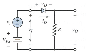
Given that VPS=9V, R=4kohm, VY = 0.6V and vi=0.2sinωt. Determine Vo and v0
Sol: For DC circuit vac=0 then the DC current is given as
IDQ = VDC-VY/R = 9-0.6/4000 = 2.1mA
The output dc component of voltage
V0=IDQ x R = 2.1x10-3 x 4000=8.4V
For AC Circuit VDC=0
Vi = idRd+idR
rd= VT/IDQ = 0.026/2.1x10-3=12.38ohm
The AC diode current is
id = Vi/rd+R = 0.2sinωt/(4000+12.38) = 49.84sinωt  A
A
The output ac voltage of circuit is
v0 = idR = 49.84sinωt  Ax4kohm = 199.38sinωt mV
Q2) A 5.0V stabilised power supply is required to be produced from a 12V DC power supply input source. The maximum power rating PZ of the Zener diode is 2W. Using the Zener regulator circuit above calculate:
a). The maximum current flowing through the Zener diode.
Maximum current = Watts/ Voltage = 2w/ 5V = 400mA
b). The minimum value of the series resistor, RS
Rs = Vs – Vz/ Iz = 2 – 5 / 400mA = 17.5 Ω
c). The load current IL if a load resistor of 1kΩ is connected across the Zener diode.
IL = Vz / RL = 5v/ 1000Ω = 5mA
d). The Zener current IZ at full load.
IZ = Is – IL = 400 mA – 5mA = 395mA
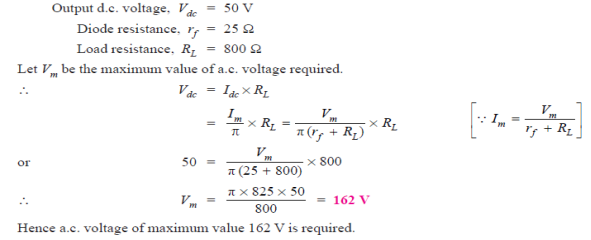
Q3) A half-wave rectifier is used to supply 50V d.c. To a resistive load of 800 Ω. The
diode has a resistance of 25 Ω. Calculate a.c. Voltage required.
Solution:
Q4) A full-wave rectifier uses two diodes, the internal resistance of each diode may
be assumed constant at 20 Ω. The transformer r.m.s. Secondary voltage from center tap to each end of secondary is 50 V and load resistance is 980 Ω. Find: (i) the mean load current (ii) the r.m.s. value of load current.
Solution:

(i) 
(ii) 
Q5) Explain Half-wave rectifier with waveforms and circuit diagram?
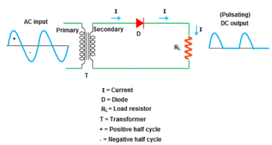
- Sol: It is the simplest form of the rectifier. Here, a single diode is used.
- It consists of an AC source, transformer (step-down), diode, and resistor (load).
- The diode is placed between the transformer and resistor (load).
Operation:
- It allows only half cycle and blocks the other half cycle.
- When it allows positive half cycles and blocks negative half cycles, it is called a positive half wave rectifier. The output DC current or DC signal produced by a positive half wave rectifier is a series of positive half cycles or positive sinusoidal pulses.
- When it allows electric current during the negative half-cycle of input AC signal and blocks electric current during the positive half-cycle of the input AC signal.
- A negative half wave rectifier produces a series of negative sinusoidal pulses.
- For an ideal diode, the positive half cycle or negative half cycle at the output is exactly same.
Characteristics of half wave rectifier
Ripple factor
The ripple factor is given as

Finally, we get
γ = 1.21
Hence, the DC voltage is 121% of the DC magnitude.
DC current
The DC current is given by,

Where,
Imax = maximum DC load current
Output DC voltage (VDC)
The output DC voltage is given by,

Where, VSmax = Maximum secondary voltage
Q6) Explain the procedure for testing a diode?
Sol:
1) Select resistance mode in the multimeter with the help of selector switch.
2) Connect negative terminal of diode with negative end of multimeter.
3) Connect positive terminal of diode with positive end of multimeter.
4) Now check the reading shown, the multimeter should show a low value of resistance, because in forward bias the diode conducts. If the reading is high then the diode is faulty. If the diode is not faulty and shown low value, we continue the testing.
5) Connect negative terminal of diode with positive end of multimeter
6) Connect positive terminal of diode with negative end of multimeter
7) Now the multimeter should show high reading as the diode is reversed biased and very low current flows. If this this the case diode is good. If the multimeter shows low readings the diode is faulty.
Q7) How does the temperature effect the diode characteristics explain?
Sol: As we already know the working of p-n junction diode. As the temperature increases the covalent bond are broken which releases many electrons and protons. This increases the amount of current flow in the diode. The diode characteristics are shown below
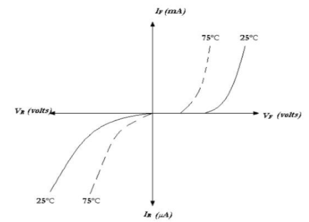
The above characteristics clearly shows that the forward characteristics are shifted upwards and reverse characteristics are shifted downwards with increase in temperature.
Q8) Explain diode approximation with necessary circuit diagram and waveforms?
Sol: In this we approximate the non-linear behaviour of the diode so that is eases the circuit analysis. Below shown are the condition for approximation.
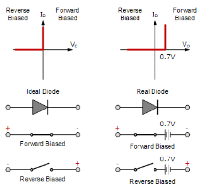
When diode is forward biased and acts a perfect conductor allowing zero potential drop is called an ideal diode. For reverse bias it acts as complete insulator.
Another approximation is when the diode id considered forward biased and connected to a battery in series. For Si diode 0.7V is required to make the diode forward biased.
For forward bias VF=VO+IFRF
For Si diode
VF=0.7+IFRF
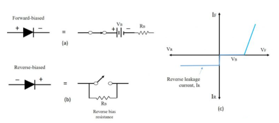
The third approximation is when the diode has voltage across it and bulk resistance RB is also connected across the diode.
The resistance will change according to the flow of current and the forward voltage through diode for any given time.
Vd = 0.7+IdRB
Q9) Explain 7-segment LED display?
Sol: The 7-segment display shows seven segments. The seven segment allows us to display decimal numbers from 0 to 9. Below shown is the 7-segment LED with its truth table.


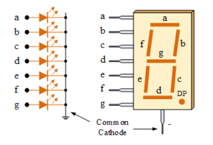
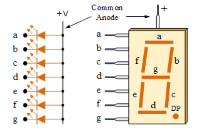
The segments can be light by forward biasing them properly in correct sequence and the other which are dark tighter make the proper desired number to be displayed. The displays common pin is generally used to identify which type of 7-segment display it is. As each LED has two connecting pins, one called the “Anode” and the other called the “Cathode”, there are therefore two types of LED 7-segment display called: Common Cathode (CC) and Common Anode (CA).
Common Cathode (CC): In this case all the cathode connections are connected to ground. The individual segment is turned ON by high logic.
Common Anode (CA): In this all the anode of LED are joined to logic 1. The individual segment is light up by applying 0 logic. These displays are generally used. For instance, to display the numerical digit 0, we will need to light up six of the LED segments corresponding to a, b, c, d, e and f.
Q10) Draw and explain IV characteristics of the PN junction diode?
Sol: When the diode is forward biased the thickness of depletion region reduces (VD>0) and the diode acts like a short circuit. There is large amount of current flowing due to this short circuit.
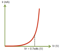
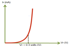
When the diode is reverse biased the thickness of depletion region increases (VD<0) and the diode acts as an open circuit. There is high voltage and no current dure to open circuit.
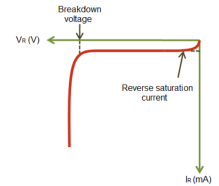
The diode current equation is given as
I=I0 ( – 1)
– 1)
I = diode current
I0 = Saturation current
Q=charge
V=Voltage applied across diode
K= Boltzmann constant=1.38x10⁻²³ JK-1
T= temperature in kelvin
For forward biased diode large amount of current flows so the above equation becomes
I=I0 ( )
)
As the current is large so 1 is neglected.
For reverse biased diode the exponential term is neglected so the current equation becomes
I=I0