Unit-4
Fabrication of Semiconductor Devices and ICs
Q1) An audio amplifier delivers 150 watts into an 8ohm speaker load when fed by a 150mW input signal. Calculate the power gain of the amplifier in decibels.
Sol: Power Gain = 10log10[P2/P1]
= 10log10[150/0.150] = 30dB
Q2) A 100watt audio amplifier has a power gain ratio of 30dB. What will be its maximum input value?
Sol: Power Gain = 10log10[P2/P1]
AP=10log10[P2/P1]
Antilog (AP/10) = 100/P1
100/P1 = 103
P1 = 100/1000 = 0.1W or 100mW
Q3) List advantages of integrated circuits?
Sol: The advantages of integrated circuits (ICs) include:
- It is quite small in size practically around 20,000 electronic components can be incorporated in a single square inch of IC chip.
- Many complex circuits are fabricated in a single chip and hence this simplifies the designing of a complex electronic circuit. Also it improves the performance.
- Reliability of ICs is high
- These are available at low cost due to bulk production.
- ICs consume very tiny power.
- Higher operating speed due to absence of parasitic capacitance effect.
- Very easily replaceable from the mother circuit.
Q4) Explain DIP packaging?
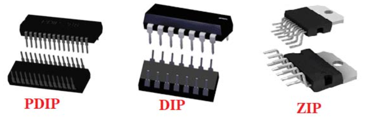
i) Sol: Dual in line package [DIP] is one of its type and most commonly used. They come in ceramic and plastic types. The number of pins ranges from 4-64. The DIP is of many types such as plastic dual in line package [PDIP] and Molded Dual in line package [MDIP]. There are zigzag in line package [ZIP] which have pins inserted perpendicular to the circuit board and are closer to each other. In standard packages the ping are 0.1” apart.

Q5) What are analog and digital ICs?
Sol: There are two types of ICs
i) Analog IC: Here both input and output signals are continuous. The output signal depends on the input signal and is linear function of input. The most common analog IC are amplifiers, comparators, timers and voltage regulators.
Ii) Digital IC: The digital IC are logic gates, microprocessors. They operate on binary data 0,1 or 0V and +5V.
Q6) How a transistor is fabricated using diffusion technique?
Sol: Diffusion Technique: In this method the N-type wafer is heated at high temperature in closed region containing vapours of P-type impurities. The p-type impurities are deposited over the N-type resulting in N-P junction. Again, the whole assembly is kept in the atmosphere of N-type vapours. The N-P junction is kept uncovered for the part which need N-type impurities to deposited, rest is covered. The vapours gets deposited on the p region forming NPN. This is explained with figure below.

Q7) List all the transistor performance parameters?
Sol: The techniques are listed below
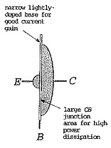
i) Current Gain: When large amount of charge carriers pass to collector through emitter current gain is high. So, the base in this case should be lightly doped and very narrow compared to emitter and collector.

Ii) High Power: For high power the transistor needs to have large E-B surface so that required amount of charge carriers can flow. As shown in above figure.
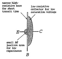
Iii) Frequency Response: For high frequency response the transistor must have very narrow base region in order to allow minimum charge carrier to flow. As for high power we need large area for EB and in this case we need narrow base junction to meet both requirements the EB junction is long thin zig-zag strip.

Iv) Switching Transistor: There has to be low junction capacitance in order to achieve fast switching. It should also have low saturation voltage and short storage time. The collector region must have low resistivity. The charge carriers in depletion region of CB junction must have faster combination to achieve short storage time.
v) Breakdown and Punch-Through: The reverse breakdown voltage is limited by the collector as CB is reverse biased. The base and collector must be lightly doped to get high breakdown voltage. The base should not be lighter than the collector because if this is the case the depletion region will penetrate into base and will cause breakdown due to punch through when connected to EB.
Q8) Explain point contact technique of fabrication?
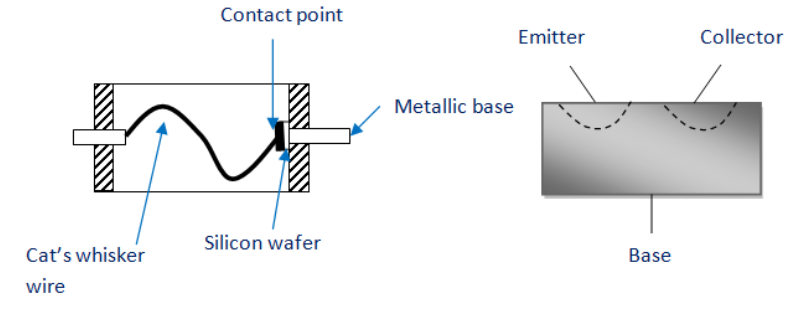
i) Sol: In this technique N-type wafer is taken its one end is soldered to metallic base and the other to the tungsten spring. Then a large amount of current is passed for a millisecond so that pn junction is created.

Q9) Explain diffusion in semiconductors?
Sol: In Diffusion an n-type semiconductor is heated in the atmosphere which has acceptor impurities present in vapour form. Due to this some of the impurities form a layer and sets on the n-type crystal. By this process p region is created on n type material. The area in which the acceptor impurity is required is left uncovered else all is covered.
Q10) How are IC categorised on the basis of transistor being used?
Sol: There are five groups of IC categorised on the basis of number of transistors being used in that IC.
i) SSI (Small Scale Integration): The number of transistors in one chip are up to 100.
Ii) MSI (Medium Scale Integration): The number of transistors in one chip are from 100-1000.
Iii) LSI (Large Scale Integration): The number of transistors in one chip are from 1000-20000.
Iv) VLSI (Very Large-Scale Integration): The number of transistors in one chip are from 20000-1000000.
v) ULSI (Ultra Large-Scale Integration): The number of transistors in one chip are from 1000000-10000000.
Unit-4
Unit-4
Fabrication of Semiconductor Devices and ICs
Q1) An audio amplifier delivers 150 watts into an 8ohm speaker load when fed by a 150mW input signal. Calculate the power gain of the amplifier in decibels.
Sol: Power Gain = 10log10[P2/P1]
= 10log10[150/0.150] = 30dB
Q2) A 100watt audio amplifier has a power gain ratio of 30dB. What will be its maximum input value?
Sol: Power Gain = 10log10[P2/P1]
AP=10log10[P2/P1]
Antilog (AP/10) = 100/P1
100/P1 = 103
P1 = 100/1000 = 0.1W or 100mW
Q3) List advantages of integrated circuits?
Sol: The advantages of integrated circuits (ICs) include:
- It is quite small in size practically around 20,000 electronic components can be incorporated in a single square inch of IC chip.
- Many complex circuits are fabricated in a single chip and hence this simplifies the designing of a complex electronic circuit. Also it improves the performance.
- Reliability of ICs is high
- These are available at low cost due to bulk production.
- ICs consume very tiny power.
- Higher operating speed due to absence of parasitic capacitance effect.
- Very easily replaceable from the mother circuit.
Q4) Explain DIP packaging?
i) Sol: Dual in line package [DIP] is one of its type and most commonly used. They come in ceramic and plastic types. The number of pins ranges from 4-64. The DIP is of many types such as plastic dual in line package [PDIP] and Molded Dual in line package [MDIP]. There are zigzag in line package [ZIP] which have pins inserted perpendicular to the circuit board and are closer to each other. In standard packages the ping are 0.1” apart.

Q5) What are analog and digital ICs?
Sol: There are two types of ICs
i) Analog IC: Here both input and output signals are continuous. The output signal depends on the input signal and is linear function of input. The most common analog IC are amplifiers, comparators, timers and voltage regulators.
Ii) Digital IC: The digital IC are logic gates, microprocessors. They operate on binary data 0,1 or 0V and +5V.
Q6) How a transistor is fabricated using diffusion technique?
Sol: Diffusion Technique: In this method the N-type wafer is heated at high temperature in closed region containing vapours of P-type impurities. The p-type impurities are deposited over the N-type resulting in N-P junction. Again, the whole assembly is kept in the atmosphere of N-type vapours. The N-P junction is kept uncovered for the part which need N-type impurities to deposited, rest is covered. The vapours gets deposited on the p region forming NPN. This is explained with figure below.

Q7) List all the transistor performance parameters?
Sol: The techniques are listed below
i) Current Gain: When large amount of charge carriers pass to collector through emitter current gain is high. So, the base in this case should be lightly doped and very narrow compared to emitter and collector.

Ii) High Power: For high power the transistor needs to have large E-B surface so that required amount of charge carriers can flow. As shown in above figure.
Iii) Frequency Response: For high frequency response the transistor must have very narrow base region in order to allow minimum charge carrier to flow. As for high power we need large area for EB and in this case we need narrow base junction to meet both requirements the EB junction is long thin zig-zag strip.

Iv) Switching Transistor: There has to be low junction capacitance in order to achieve fast switching. It should also have low saturation voltage and short storage time. The collector region must have low resistivity. The charge carriers in depletion region of CB junction must have faster combination to achieve short storage time.
v) Breakdown and Punch-Through: The reverse breakdown voltage is limited by the collector as CB is reverse biased. The base and collector must be lightly doped to get high breakdown voltage. The base should not be lighter than the collector because if this is the case the depletion region will penetrate into base and will cause breakdown due to punch through when connected to EB.
Q8) Explain point contact technique of fabrication?
i) Sol: In this technique N-type wafer is taken its one end is soldered to metallic base and the other to the tungsten spring. Then a large amount of current is passed for a millisecond so that pn junction is created.

Q9) Explain diffusion in semiconductors?
Sol: In Diffusion an n-type semiconductor is heated in the atmosphere which has acceptor impurities present in vapour form. Due to this some of the impurities form a layer and sets on the n-type crystal. By this process p region is created on n type material. The area in which the acceptor impurity is required is left uncovered else all is covered.
Q10) How are IC categorised on the basis of transistor being used?
Sol: There are five groups of IC categorised on the basis of number of transistors being used in that IC.
i) SSI (Small Scale Integration): The number of transistors in one chip are up to 100.
Ii) MSI (Medium Scale Integration): The number of transistors in one chip are from 100-1000.
Iii) LSI (Large Scale Integration): The number of transistors in one chip are from 1000-20000.
Iv) VLSI (Very Large-Scale Integration): The number of transistors in one chip are from 20000-1000000.
v) ULSI (Ultra Large-Scale Integration): The number of transistors in one chip are from 1000000-10000000.