UNIT-1
Semiconductor Diode
Q1) What is depletion layer? Explain using PN junction diode.
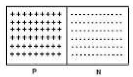
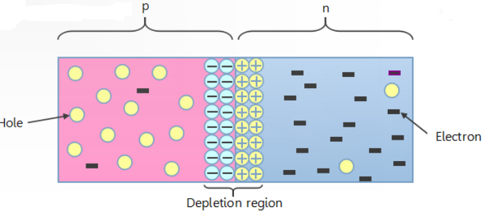
A1) When a semi-conductor is doped such that half the portion is doped with the trivalent impurity (Al, Ar, Bi) and the other half is doped with pentavalent impurity (B, P) then the junction formed is known as PN junction.
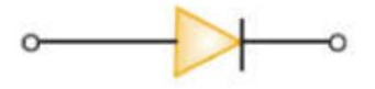
Its symbol is
Depletion layer
At normal condition, the holes from P region diffuse into N region and electrons from N region diffuse in P region.
A thin layer of positive ion is formed in the N region and negative ions in the P region near the junction are formed.
This thin layer that is formed is known as depletion layer.
Q2) Draw and explain reverse biasing.
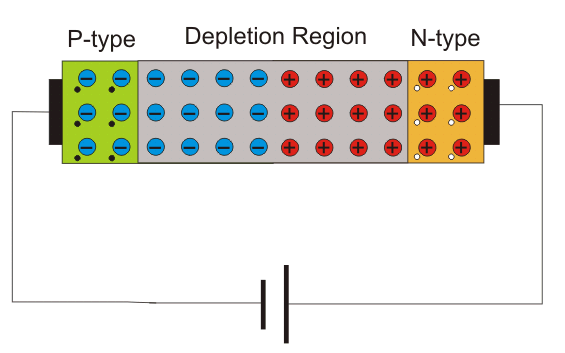
A2) When positive terminal is connected to the n-type region and the negative terminal is connected to the p-type region then the pn junction is said to be in reverse biased condition.
When no voltage applied across the p n junction, the potential developed across the junction is 0.3 volts at 25oC for germanium and 0.7 volts at 25oC for silicon p n junction.
The polarity of this potential barrier is same as the polarity of voltage source applied during reverse biased condition.
Now if reverse biased voltage is increased the barrier potential developed also increases. Hence, the pn junction widens.
The free electrons of the n-type region are attracted towards positive terminal of the source because of that more positive impurity ions are created in the depletion layer which makes the layer thicker.
At the same time, electrons are injected in the p-type region. Due to the positive potential of the n-type region the electrons are drifted towards the junction and combine with holes and create more positive impurity ions in the layer.
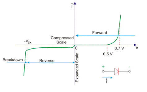
Q3) Draw and explain I-V characteristics of PN junction diode.
A3)
Q4) Explain types of capacitance in detail.
A4) Diode Capacitance
The ability of the material to store electric charge is called capacitance.
The change of capacitance at the depletion region can be defined as the change in electric charge per change in voltage.
CT = dQ / dV
Where,
CT = Transition capacitance
dQ = Change in electric charge
dV = Change in voltage
Transition Capacitance
The amount of capacitance changes with increase in voltage is called transition capacitance.
The transition capacitance is also known as depletion region capacitance, junction capacitance or barrier capacitance. Transition capacitance is denoted as CT.
The transition capacitance can be mathematically written as,
CT = ε A / W
Where,
ε = Permittivity of the semiconductor
A = Area of plates or p-type and n-type regions
W = Width of depletion region
Diffusion capacitance (CD)
It occurs in a forward biased p-n junction diode.
It is also referred as storage capacitance. It is denoted as CD.
Diffusion capacitance is given by,
CD = dQ / dV
Where,
CD = Diffusion capacitance
dQ = Change in number of minority carriers stored outside the depletion region
dV = Change in voltage applied across diode
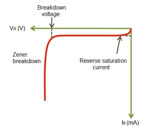
Q5) Draw and explain zener diode in detail.
A5) A zener diode is a special type of device designed to operate in the zener breakdown region.
It acts like normal p-n junction diode under forward bias condition. When forward biased voltage is applied, it allows large amount of electric current and blocks only a small amount.
It is heavily doped than the normal p-n junction diode. Hence, it has very thin depletion region. Hence, allows more electric current than the normal p-n junction diodes.
It allows electric current in the reverse direction if the applied reverse voltage is greater than the zener voltage.
It is always connected in reverse direction because it is specifically designed to work in reverse direction.
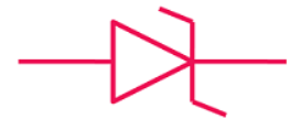
Symbol
V-I characteristics
Q6) Write short note on photo diode.
A6) A photodiode is a p-n junction or pin semiconductor device that consumes light energy to generate electric current. It is also sometimes referred as photo-detector, photo-sensor, or light detector.
Photodiodes are specially designed to operate in reverse bias condition. Reverse bias means that the p-side of the photodiode is connected to the negative terminal of the battery and n-side is connected to the positive terminal of the battery.
Photodiode is very sensitive to light so when light or photons falls on the photodiode it easily converts light into electric current. Solar cell is also known as large area photodiode because it converts solar energy or light energy into electric energy.
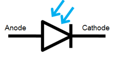
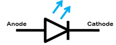
Symbol
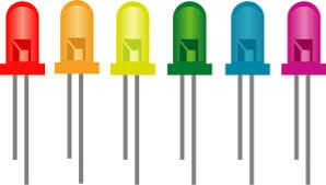
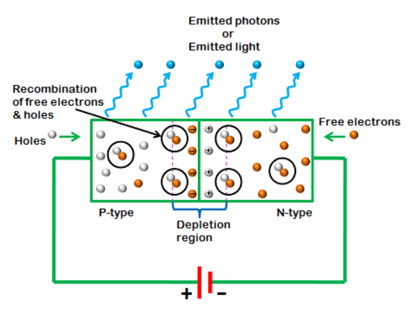
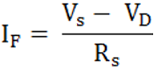
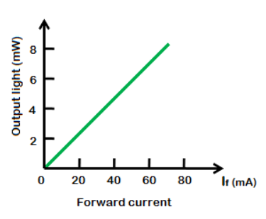
Q7) Draw and explain LED in detail.
A7)

The current flowing through the LED is mathematically written as
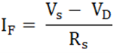
Where,
IF = Forward current
VS = Source voltage or supply voltage
VD = Voltage drop across LED
RS = Resistor or current limiting resistor
Symbol
Output characteristics of LED
Q8) What are the advantages and disadvantages of center tapped full-wave rectifiers compared with Bridge rectifiers?
Center tapped FWR | Bridge Recticfier |
One diode conducts in each half cycle of input | Two diodes conduct in each half cycle of input |
The output voltage is more | The output voltage is less |
PIV rating of the diode is 2Vsm | PIV rating of the diode is Vsm |
The transformer is less effectively used T.U.F is 0.693. | The transformer is more effectively used T.U.F is 0.812. |
Q9) Explain Clipper and its types in detail.
A9) Clippers are networks that employ diodes to “clip” away a portion of an input signal without distorting the remaining part of the applied waveform.
Positive Diode Clipping Circuits
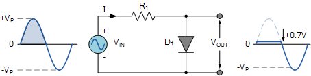
In this, the diode is forward biased during the positive half cycle of the sinusoidal input waveform. For this, it must have the input voltage magnitude greater than +0.7 volts (0.3 volts for a germanium diode).
When this happens, the diodes begins to conduct and holds the voltage across itself until the sinusoidal waveform falls below the value. Thus, the output voltage taken across the diode can never exceed 0.7 volts during the positive half cycle.
During the negative half cycle, the diode is reverse biased blocking current flow through itself and thus has no effect on the negative half of the sinusoidal voltage which passes to the load unaltered. Thus, the diode limits the positive half of the input waveform and is known as a positive clipper circuit.
Negative Diode Clipping Circuits
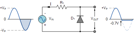
Here the reverse happens. The diode is forward biased during the negative half cycle of the sinusoidal waveform and limits or clips it to –0.7 volts while allowing the positive half cycle to pass unaltered when reverse biased.
As the diode limits the negative half cycle of the input voltage it is therefore called a negative clipper circuit.
Clipping of Both Half Cycles
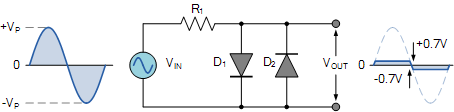
If the two diodes are connected in inverse parallel, then both the positive and negative half cycles would be clipped as diode D1 clips the positive half cycle of the sinusoidal input waveform while diode D2 clips the negative half cycle.
Hence, diode clipping circuits can be used to clip the positive half cycle, the negative half cycle or both.
For ideal diodes the output waveform above would be zero. However, due to the forward bias voltage drop across the diodes the actual clipping point occurs at +0.7 volts and –0.7 volts respectively.
Q10) Explain Clamper and its types in detail.
A10) A clamper is a network constructed of a diode, a resistor, and a capacitor that shifts a waveform to a different dc level without changing the appearance of the applied signal.
The positive or negative peak of a signal can be positioned at the desired level by using the clamping circuits. As we can shift the levels of peaks of the signal by using a clamper, hence, it is also called as level shifter.
The clamper circuit consists of a capacitor and diode connected in parallel across the load. The clamper circuit depends on the change in the time constant of the capacitor. The capacitor must be chosen such that, during the conduction of the diode, the capacitor must be sufficient to charge quickly and during the non-conducting period of diode, the capacitor should not discharge drastically. The clampers are classified as positive and negative clampers based on the clamping method.
Negative Clamper
During the positive half cycle, the input diode is in forward bias and as the diode conducts, capacitor gets charged. During the negative half cycle, the output voltage become equal to the sum of the input voltage and the voltage stored across the capacitor.
Positive Clamper
It is similar to the negative clamper circuit, but the diode is connected in the opposite direction. During the positive half cycle, the voltage across the output terminals becomes equal to the sum of the input voltage and capacitor voltage. During the negative half cycle, the diode starts conducting and charges the capacitor rapidly to its peak input value. Thus, the waveforms are clamped towards the positive direction.
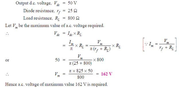
Q11) A half-wave rectifier is used to supply 50V d.c. to a resistive load of 800 Ω. The
diode has a resistance of 25 Ω. Calculate a.c. voltage required.
A11)
Q12) A full-wave rectifier uses two diodes, the internal resistance of each diode may
be assumed constant at 20 Ω. The transformer r.m.s. secondary voltage from centre tap to each end of secondary is 50 V and load resistance is 980 Ω. Find : (i) the mean load current (ii) the r.m.s. value of load current.
A12)
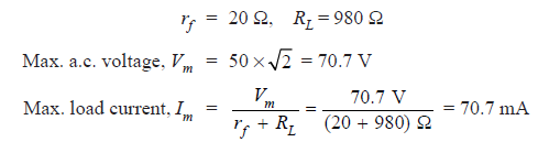
(i) 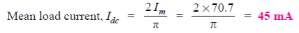
(ii) 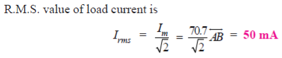
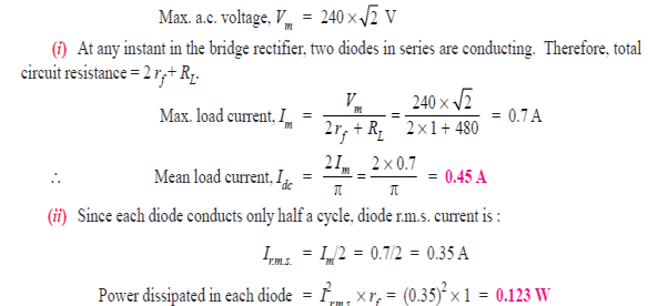
Q13) The four diodes used in a bridge rectifier circuit have forward resistances which may be considered constant at 1Ω and infinite reverse resistance. The alternating supply voltage is 240 V r.m.s. and load resistance is 480 Ω. Calculate (i) mean load current and (ii) power dissipated in each diode.
A13)
Q14) Write short note on: LCD and tunnel diode.
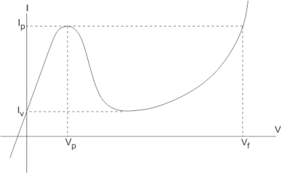
A14) Tunnel diode
A tunnel diode (also known as a Esaki diode) is a type of semiconductor diode that has effectively “negative resistance” due to the quantum mechanical effect called tunneling. Tunnel diodes have a heavily doped pn junction that is about 10 nm wide. The heavy doping results in a broken band gap, where conduction band electron states on the N-side are more or less aligned with valence band hole states on the P-side.
The application of transistors in a very high in frequency range are hampered due to the transit time and other effects. Many devices use the negative conductance property of semiconductors for these high frequency applications. A tunnel diode is one of the most commonly used negative conductance devices. It is also known as Esaki diode after L. Esaki for his work on this effect.
The concentration of dopants in both p and n region is very high, at around 1024 – 1025 m-3. The pn junction is also abrupt. For this reasons, the depletion layer width is very small. In the current voltage characteristics of tunnel diode, we can find a negative slope region when a forward bias is applied.
The name “tunnel diode” is due to the quantum mechanical tunneling is responsible for the phenomenon that occurs within the diode. The doping is very high so at absolute zero temperature the Fermi levels lies within the bias of the semiconductors.
Characteristics of Tunnel Diode
When reverse bias is applied the Fermi level of the p-side becomes higher than the Fermi level of n-side. Hence, the tunneling of electrons from the balance band of p-side to the conduction band of n-side takes place. With the interments of the reverse bias the tunnel current also increases.
When forward bias is applied the Fermi level of n-side becomes higher that the Fermi level of p-side, thus the tunneling of electrons from the n-side to p-side takes place. The amount of the tunnel current is very large than the normal junction current. When the forward bias is increased, the tunnel current is increased up to certain limit.
When the band edge of n-side is the same as the Fermi level in p-side, the tunnel current is maximum with the further increment in the forward bias the tunnel current decreases and we get the desired negative conduction region. When the forward bias is raised further, normal pn junction current is obtained which is exponentially proportional to the applied voltage. The V-I characteristics of the tunnel diode is given,
The negative resistance is used to achieve oscillation and often Ck+ function is of very high frequency frequencies.
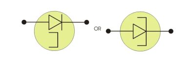
Tunnel Diode Symbol
The symbol for a tunnel diode is shown below.
LCD
LCD (Liquid Crystal Display) is a type of flat panel display which uses liquid crystals in its primary form of operation. LEDs have a large and varying set of use cases for consumers and businesses, as they can be commonly found in smartphones, televisions, computer monitors and instrument panels.
LCDs were a big leap in terms of the technology they replaced, which include light-emitting diode (LED) and gas-plasma displays. LCDs allowed displays to be much thinner than cathode ray tube (CRT) technology. LCDs consume much less power than LED and gas-display displays because they work on the principle of blocking light rather than emitting it. Where an LED emits light, the liquid crystals in an LCD produces an image using a backlight.
As LCDs have replaced older display technologies, LCDs have begun being replaced by new display technologies such as OLEDs.
How LCDs work
A display is made up of millions of pixels. The quality of a display commonly refers to the number of pixels; for example, a 4K display is made up of 3840 x2160 or 4096x2160 pixels. A pixel is made up of three subpixels; a red, blue and green—commonly called RGB. When the subpixels in a pixel change color combination, a different color can be produced. With all the pixels on a display working together, the display can make millions of different colors. When the pixels are rapidly switched on and off, a picture is created.
The way a pixel is controlled is different in each type of display; CRT, LED, LCD and newer types of displays all control pixels differently. In short, LCDs are lit by a backlight, and pixels are switched on and off electronically while using liquid crystals to rotate polarized light. A polarizing glass filter is placed in front and behind all the pixels, the front filter is placed at 90 degrees. In between both filters are the liquid crystals, which can be electronically switched on and off.
LCDs are made with either a passive matrix or an active-matrix display grid. The active-matrix LCD is also known as a thin film transistor (TFT) display. The passive matrix LCD has a grid of conductors with pixels located at each intersection in the grid. A current is sent across two conductors on the grid to control the light for any pixel. An active matrix has a transistor located at each pixel intersection, requiring less current to control the luminance of a pixel. For this reason, the current in an active-matrix display can be switched on and off more frequently, improving the screen refresh time.
Some passive matrix LCD's have dual scanning, meaning that they scan the grid twice with current in the same time that it took for one scan in the original technology. However, active matrix is still a superior technology out of the two.


